Showing posts with label portable. Show all posts

Thursday, November 13, 2014

Lamp Flasher Portable circuit

 lamp flasher portable circuit
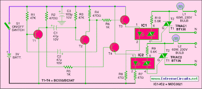
Here is a portable, high-power incandescent electric lamp flasher. It is basically a dual flasher (alternating blinker) that can handle two separate 230V AC loads (bulbs L1 and L2). The circuit is fully transistorised and battery-powered. The free-running oscillator circuit is realised using two low-power, low-noise transistors T1 and T2. One of the two transistors is always conducting, while the other is blocking.

Due to regular charging and discharging of capacitors C1 and C2, the two transistors alternate between conduction and non-conduction states. The collector of transistor T1 is connected to the base of driver transistor T4 through current-limiting resistor R5. Similarly, the collector of transistor T2 is connected to the base of driver transistor T3 through limiting resistor R6. These transistors are used to trigger Triac1 and Triac2 (each BT136) through optotriacs IC1 and IC2, respectively, and switch on the power supply to external loads L1 and L2.
IC1 and IC2 operate alternatively at a low frequency determined by the values of capacitors C1 and C2. The oscillator circuit built around transistors T1 and T2 generates low frequencies. When transistor T3 conducts, IC1 is enabled to ire Triac1 and bulb L1 glows. Similarly, when transistor T4 conducts, IC2 is enabled to ire Triac2 and bulb L2 glows. Connect the power supply line (L) of mains to bulbs L1 and L2, and neutral (N) to T1 terminals of Triac1 and Triac2.


You can also connect neutral (N) line of the external 230V mains supply to both loads (bulbs L1 and L2) as a common line and then route supply line (L) to respective loads (bulbs L1 and L2). The circuit works off only 3 volts. Since current consumption is fairly low, two AA-type cells are suficient to power the circuit. Assemble the circuit on a general-purpose PCB and enclose in a suitable plastic cabinet with integrated AA-size pen-light cell holder. Drill holes for mounting the ‘on’/‘off’ switch and power switching terminals. Also connect two bulb holders for bulbs L1 and L2.

Tuesday, November 4, 2014

Portable 9v Headphone Amplifier

High Quality One-IC unit, Low current consumption. After several requests by correspondents, the decision of designing a 9V powered Headphone Amplifier was finally taken. The main requirement was to power the circuit by means of a common, PP3 (transistor radio) alkaline battery. So, implementing a low current drawing circuit was absolutely necessary, though preserving a High Quality performance.

Portable 9v Headphone Amplifier Circuit Diagram
Portable

Parts:
P1 = 22K
R1 = 18K
R2 = 68K
R3 = 68K
R4 = 68K
R5 = 18K
R6 = 68K
C1 = 4.7uF-25v
C2 = 4.7uF-25v
C3 = 22pF
C4 = 220uF-25v
C5 = 220uF-25v
C6 = 4.7uF-25v
C7 = 22pF
C8 = 220uF-25v
J1 = 3.5mm Stereo Jack
B1 = 9V Alkaline Battery
IC1 = NE5532-34
SW1 = SPST Toggle Switch

The appearance of the 5534 low-noise op-amp at a reasonable price was much appreciated by audio designers. It is now difficult or impossible to design a discrete stage that has the performance of the 5534 without quite unacceptable complexity. 5534 op-amps are now available from several sources, in a conventional 8-pin d.i.l. format. This version is internally compensated for gains of three or more, but requires a small external capacitor (5-15pF) for unity-gain stability. The 5532 is a very convenient package of two 5534s in one 8-pin device with internal unity-gain compensation, as there are no spare pins.

The 5534/2 is a low-distortion, low-noise device, having also the ability to drive low-impedance loads to a full voltage swing while maintaining low distortion. Furthermore, it is fully output short-circuit proof. Therefore, this circuit was implemented with a single 5532 chip forming a pair of stereo, inverting amplifiers, having an ac gain of about 3.5 and capable of delivering up to 3.6V peak-to-peak into a 32 Ohm load (corresponding to 50mW RMS) at less than 0.025% total harmonic distortion (1kHz & 10kHz). If we consider that the mean current drawing at a power output of 15mW per channel is around 12-13mA (both channels driven), this Headphone Amplifier will become a must for many DIY enthusiasts needing a High Quality, High Performance portable device.

Technical data
Sensitivity:
    200mV RMS for 15.6mW RMS output
    350mV RMS for 50mW RMS output
Maximum undistorted output: 3.6V Peak-to-peak
Frequency response: flat from 40Hz to 20KHz; -2.3dB @ 20Hz
Total harmonic distortion @ 1KHz: <0.025% at all power outputs up to 50mW RMS
Total harmonic distortion @10KHz: <0.02% at all power outputs up to 50mW RMS
Total current drawing @ 9V supply (both channels driven):
    Standing current: 8.5mA
    Mean current drawing @ 15mW RMS per channel: 12mA
    Mean current drawing @ 35mW RMS per channel: 17mA


Wednesday, September 24, 2014

New 4 Channel Portable Audio Mixer

The target of this project was the design of a small portable mixer supplied by a 9V PP3 battery, keeping high quality performance. The mixer is formed assembling three main modules that can be varied in number and/or disposition to suit everyone needs. The three main modules are:

Input Amplifier Module: a low noise circuit equipped with a variable voltage-gain (10 - 100) preset, primarily intended as high quality microphone input, also suitable for low-level line input.

Tone Control Module: a three-band (Bass, Middle, Treble) tone control circuit providing unity-gain when its controls are set to flat frequency response. It can be inserted after one or more Input Amplifier Modules and/or after the Main Mixer Amplifiers.

Main Mixer Amplifier Module: a stereo circuit incorporating two virtual-earth mixers and showing the connection of one Main Fader and one Pan-Pot.

The image below shows a Block diagram of the entire mixer featuring four Input Amplifier Modules followed by four in-out switchable Tone Control Modules, one stereo Line input, four mono Main Faders, one stereo dual-ganged Main Fader, four Pan-Pots, a stereo Main Mixer Amplifier Module and two further Tone Control Modules switchable in and out for each channel, inserted before the main Left and Right outputs.

Obviously this layout can be rearranged at everyone wish. An astonishing feature of this design lies in the fact that a complete stereo mixer as shown below in the Block diagram draws less than 6mA current!

Block diagram:

4 channel input mixer

Input Amplifier Module
Circuit Diagram:

Parts:

R1 = 22K - 1/4W Resistor
R2 = 22K - 1/4W Resistor
R3 = 47K - 1/4W Resistor
R4 = 47K - 1/4W Resistor
R5 = 47K - 1/4W Resistor
R6 = 4K7 - 1/4W Resistor
R7 = 22K - 1/4W Resistor
R8 = 220R - 1/4W Resistor
R9 = 2K - 1/2W Trimmer Cermet (See Notes)
R10 = 470K - 1/4W Resistor
R11 = 560R - 1/4W Resistor
R12 = 100K - 1/4W Resistor
R13 = 220R - 1/4W Resistor

C1 = 470nF - 63V Polyester Capacitor
C2 = 100µF - 25V Electrolytic Capacitor
C3 = 2µ2 - 63V Electrolytic Capacitor
C4 = 2µ2 - 63V Electrolytic Capacitor
C5 = 2µ2 - 63V Electrolytic Capacitor
C6 = 47pF - 63V Ceramic Capacitor
C7 = 4µ7 - 63V Electrolytic Capacitor
C8 = 100µF - 25V Electrolytic Capacitor
Q1 = BC560C - 45V 100mA Low noise High gain PNP Transistor
Q2 = BC550C - 45V 100mA Low noise High gain NPN Transistor
IC1 = TL061 - Low current BIFET Op-Amp

Circuit Description:

The basic arrangement of this circuit is derived from the old Quad magnetic pick-up cartridge module. The circuit was rearranged to cope with microphone input and a single-rail low voltage supply. This low-noise, fully symmetrical, two-transistor head amplifier layout, allows the use of a normal FET input Op-Amp as the second gain stage, even for very sensitive microphone inputs. The voltage-gain of this amplifier can be varied by means of R9 from 10 to 100, i.e. 20 to 40dB.

Notes:
  • R9 can be a trimmer, a linear potentiometer or a fixed-value resistor at will.
  • When voltage-gain is set to 10, the amplifier can cope with 800mV peak-to-peak maximum Line levels.
  • Current drawing for one Input Amplifier Module is 600µA.
  • Frequency response is 20Hz to 20KHz - 0.5dB.
  • Total Harmonic Distortion measured with voltage-gain set to 100: 2V RMS output = <0.02%>
  • Total Harmonic Distortion measured with voltage-gain set to 10 & 33: 2V RMS output = <0.02%>
  • THD is much lower @ 1V RMS output.
  • Maximum undistorted output voltage: 2.8V RMS.