Showing posts with label circuit. Show all posts

Thursday, November 20, 2014

SMS Remote controller circuit

SMS Remote controller is a device used to control a device remotely using SMS through GSM mobile phones. Process control equipment with a series of AVR ATTiny To SMS Remote Controller can be used to control life and death of these equipment will provide information on the status of replies to our phone in return successful command execution. 
Equipment can be controlled by a series of AVR ATTiny To SMS Remote Controller include lights, water pumps, garage doors, gates and much more. AVR series ATTiny To SMS Remote controller uses the module-47 Sony ericson GM as recipient and sender of the SMS module. Then to the SMS data processor on a series of AVR ATTiny To SMS Remote controller is using AVR microcontroller ATTiny 2313.


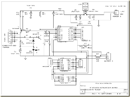
Series AVR ATTiny To SMS Remote Controller

SMS Remote controller circuit Click to view larger. 

AVR circuit this part ATTiny To SMS Remote Controller
AVR series ATTiny To SMS Remote controller uses the AVR attiny2313 with 4MHz clock frequency, GSM Module GM trnceiver 47 Sony ericson, SIM Card, 4 relays and an IC regulator. ATTiny AVR microcontroller 2313 can work well on the voltage 2.7 VDC - 5.5 VDC for working with the frequency at 10MHz bahwah. 

The set of AVR ATTiny In SMS Remote Controller To make use of this power supply from the batteries 3.3 VDC. Connection using a SIM Card SIM Card Holder which is connected to the module GM-47, AVR series ATTiny To SMS Remote Controller works with communication between AVR ATTiny and GM-47 module at 9600bps. In a series of AVR ATTiny To SMS Remote controller is equipped with LED D6 as an indicator of the data interconnect GM-47 module with cellular operators where this LED will light continuously when not apat network and will be lit by flashes when a signal from the operator.

Specifications AVR series ATTiny To SMS Remote Controller
  • 4 Relay for ON / OFF electronic devices
  • 8 input lines for reading in a normal switching
  • LED indicators signal operator
  • SMS command with password, so only the owner can operate

Guitar Amplifier Circuit Diagram 100W

GuitarGuitar Amplifier Circuit Diagram 100W

The ability amp lath has remained banausic back it was aboriginal appear in 2002. It absolutely isn’t broken, so there’s no acumen to fix it. The photo beneath shows a absolutely accumulated lath (available as apparent as M27). Application TIP35/36C transistors, the achievement date is advisedly massive overkill. This ensures believability beneath the best backbreaking date conditions. No amplifier can be fabricated allowed from everything, but this does appear close.

The ability amp (like the antecedent version) is about based on the 60 Watt amp ahead appear (Project 03), but it has added accretion to bout the preamp. Other modifications accommodate the abbreviate ambit aegis – the two little groups of apparatus abutting to the bent diodes (D2 and D3). This new adaptation is not massively altered from the original, but has adjustable bias, and is advised to accommodate a “constant current” (i.e. aerial impedance) achievement to the speakers – this is accomplished application R23 and R26. Note that with this arrangement, the accretion will change depending on the amount impedance, with lower impedances giving lower ability amp gain. This is not a problem, so may cautiously be ignored.

Should the achievement be shorted, the connected accepted achievement appropriate will accommodate an antecedent akin of protection, but is not absolutely foolproof. The abbreviate ambit aegis will absolute the achievement accepted to a almost safe level, but a abiding abbreviate will account the achievement transistors to abort if the amp is apprenticed hard. The aegis is advised not to accomplish beneath accustomed conditions, but will absolute the aiguille achievement accepted to about 8.5 Amps. Beneath these conditions, the centralized fuses (or the achievement transistors) will apparently draft if the abbreviate is not detected in time.

Wednesday, November 19, 2014

Turbo Bass Circuit

Turbo
Turbo Bass Circuit

Tuesday, November 18, 2014

Guitar Control Circuit Diagram

GuitarGuitar Control Circuit Diagram

Device purpose:

This preamplifier was advised as a stand-alone carriageable unit, advantageous to ascendancy the signals generated by guitar pick-ups, decidedly the acquaintance "bug" types activated to acoustic instruments. Obviously it can be acclimated with any blazon of apparatus and pick-up.

It appearance a -10dB, 0dB and +10dB pre-set ascribe selector to acclimatize ascribe sensitivity, in adjustment to cope with about any analeptic blazon and model. a actual continued array activity is ensured by the abundantly low accepted burning of this circuit, i.e. beneath than 800µA.

Circuit operation:

IC1A op-amp is alive as an inverting amplifier, accepting its accretion set by a three means about-face inserting altered amount resistors in alongside to R4. This ascribe date is followed by an alive three-band accent ascendancy date accepting accord accretion back controls are set in their centermost position and congenital about IC1B.

Monday, November 17, 2014

Loudspeaker Driver Circuit

The series of loudspeaker drivers are electronic circuits that function to bridge between high-output circuit with a loudspeaker berimpedasi berimpedansi low. 


Loudspeaker

Why this driver is needed so that the output voltage to be inserted into the loudspeaker is not impaired. Declining value of this voltage is very possible given the lack of rules regarding the distribution of voltage and resistance instead of parallel. Where every prisoner that is placed parallel with other prisoners or the inmates totally substitute for detainee custody is smaller than with individual prisoners themselves. For example, 10 ohm resistance 10 ohms paralleled with the prisoners would get custody instead of 5 ohms. Resistivity 10 ohm to 100,000 ohm paralleled the total resistance is 9.9990 ohms. So it can be concluded that the total voltage will always be smaller than the origin of each detainee. Then, with a decrease in resistance (only using a combination of resistors) or the impedance of the output terminals before, then in accordance with the laws of the voltage divider in series can be ascertained that the prisoners connect in series with output terminal will have a larger part of the voltage and output terminal itself will decline voltage.

The working principle speaker driver circuit is actually very simple and easy to understand. Where the input signal is only used as a trigger to move the second driver transistor to the rhythm of the input signal. While the current that would flow to the loudspeaker most of the power supply driver circuit. You could say similar to the use of transistors as switches. Therefore, in this speaker series driver not found a combination of resistors for reinforcement. So if we look at the picture above, so most of the current flowing in the loudspeaker load is derived from the 9 volt supply voltage, instead of the input ac signal, so that the input signal will not be burdened.

System circuit not Minimum Evaluation Board AT89C2051 and AT89C4051

Maybe we are more familiar with the term Minimum System AT89C2051 circuit, but this time I present a circuit which is not only a series of Minimum System AT89C2051 but more than that.
System

The circuit is more deserves to be called Evaluation Board AT89C2051 and AT89C4051. Some of the advantages of circuit Minimum System AT89C2051 / AT89C2051 and AT89C4051 Evaluation Board which I was present this time, hardware-hardware support below:


RS-232 interface, DB-9
Header for LCD display
I2C, PCF8574 I / O extender
AT24C04, I2C EEPROM

Friday, November 14, 2014

DC MOTOR REVERSING CIRCUIT

When the forward button is pressed and released the motor will run continuously in one direction. The reverse button will cause the motor to run continuously in the opposite direction. The motor cannot be switched from forward to reverse unless the stop switch is pressed first and vice versa. Putting a motor straight into reverse would be quite dangerous, because when running a motor develops a back emf voltage which would add to current flow in the opposite direction and probably cause arcing of the relay contacts.

Circuit Diagram


Note

At first glance this may look over-complicated, but this is simply because three non-latching push button switches are used. When the forward button is pressed and released the motor will run continuously in one direction. The Stop button must be used before pressing the reverse button. The reverse button will cause the motor to run continuously in the opposite direction, or until the stop button is used. Putting a motor straight into reverse would be quite dangerous, because when running a motor develops a back emf voltage which would add to current flow in the opposite direction and probably cause arcing of the relay contacts. This circuit has a built-in safeguard against that condition. 

Circuit Operation 

Assume that the motor is not running and that all relays are unenergized. When the forward button is pressed, a positive battery is applied via the NC contacts of B1 to the coil of relay RA/2. This will operate as the return path is via the NC contacts of D1. Relay RA/2 will operate. Contacts A1 maintain power to the relay even though the forward button is released.
Contacts A2 apply power to the motor which will now run continuously in one direction. If now the reverse button is pressed, nothing happens because the positive supply for the switch is fed via the NC contact A1, which is now open because Relay RA/2 is energized. To Stop the motor the Stop switch is pressed, Relay D operates and its contact D1 breaks the power to relays A and B, (only Relay A is operated at the moment). If the reverse switch is now pressed and released. Relay B operates via NC contact A1 and NC contact D1. Contact B1 closes and maintains power so that the relay is now latched, even when the reverse switch is opened. Relay RC/2 will also be energized and latched. Contact B2 applies power to the motor but as contacts C1 and C2 have changed position, the motor will now run continuously in the opposite direction. Pressing the forward button has no effect as power to this switch is broken via the now open NC contact B1. If the stop button is now pressed. Relay D energizes, its contact D1 breaks power to relay B, which in turn breaks power to relay C via the NO contact of B1 and of course the motor will stop. All very easy. The capacitor across relay D is there to make sure that relay D will operate at least longer than the time relays A,B and C take to release.

Correction to Diagram

In the original circuit when the Stop switch was pressed, relay RA remains energized, its holding current path is through relay coils RB and RC. To fix this relay D has two contacts, D2 now breaks power to the relay coil.

Thursday, November 13, 2014

555 timer bassed Metal detector circuit with explanation

A very simple metal detector electronic project can be designed using a simple 555 timer integrated circuit . As you can see in the schematic circuit , this electronic project requires few external electronic parts .

This circuit detects metal and also magnets. When a magnet is brought close to the 10mH choke, the output frequency changes.
This metal detector project can be powered from a power supply that can provide an output DC voltage between 6 an 12 volt .
If a metal is closer to the L1 coil , will produce a change of output oscillation frequency, that will generate a sound in the 8 ohms speaker .

Metal

readmore: electroniq.net/other-projects/detectors/metal-detector-using-555-timer-circuit.html

Lamp Flasher Portable circuit

 lamp flasher portable circuit
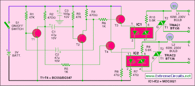
Here is a portable, high-power incandescent electric lamp flasher. It is basically a dual flasher (alternating blinker) that can handle two separate 230V AC loads (bulbs L1 and L2). The circuit is fully transistorised and battery-powered. The free-running oscillator circuit is realised using two low-power, low-noise transistors T1 and T2. One of the two transistors is always conducting, while the other is blocking.

Due to regular charging and discharging of capacitors C1 and C2, the two transistors alternate between conduction and non-conduction states. The collector of transistor T1 is connected to the base of driver transistor T4 through current-limiting resistor R5. Similarly, the collector of transistor T2 is connected to the base of driver transistor T3 through limiting resistor R6. These transistors are used to trigger Triac1 and Triac2 (each BT136) through optotriacs IC1 and IC2, respectively, and switch on the power supply to external loads L1 and L2.
IC1 and IC2 operate alternatively at a low frequency determined by the values of capacitors C1 and C2. The oscillator circuit built around transistors T1 and T2 generates low frequencies. When transistor T3 conducts, IC1 is enabled to ire Triac1 and bulb L1 glows. Similarly, when transistor T4 conducts, IC2 is enabled to ire Triac2 and bulb L2 glows. Connect the power supply line (L) of mains to bulbs L1 and L2, and neutral (N) to T1 terminals of Triac1 and Triac2.


You can also connect neutral (N) line of the external 230V mains supply to both loads (bulbs L1 and L2) as a common line and then route supply line (L) to respective loads (bulbs L1 and L2). The circuit works off only 3 volts. Since current consumption is fairly low, two AA-type cells are suficient to power the circuit. Assemble the circuit on a general-purpose PCB and enclose in a suitable plastic cabinet with integrated AA-size pen-light cell holder. Drill holes for mounting the ‘on’/‘off’ switch and power switching terminals. Also connect two bulb holders for bulbs L1 and L2.

Clap Switch Circuit Project

This is a simple electronics circuit of clap switch project. If you are a beginner electronics learner, and love to get new project experiment then this is a great circuit for you.  This circuit can on/off a 220V electronic device like fan, lamp by the sound of clap.

Circuit diagram of clap switch

clap-switch

Circuit Description

As shown in the circuit a very few number of parts is used including relay, transformer, condenser microphone, few transistor, a lamp etc. Lamp is used as a testing device; here another device could be use like fan, calling bell, radio etc.

The basic principle applied in this circuit: 
“Clap sound is being converted into electrical signal and a relay gets triggered from it and controls the load.”

A small microphone (MIC) detects the clap sound and converts into electrical signal. Which is amplified by Q1 (here Q1 used as a common emitter amplifier). Amplified signal goes into the Bistable Multivibrator section made by two transistors Q2 and Q3.

When we apply a trigger to the Bistable Multivibrator circuit with a clap sound then, if Q2 is on, Q3 gets switched off. Thus, the circuit remains stable in a single state continuously. At the moment if we trigger with another clap sound the two states will flip-flop with Q2 switched off and Q3 switched on. The circuit will remain stable continuously until we apply the next trigger.

Relay gets triggered from the output of current-amplifier (Q4) which is used to amplify the flip-flop signal. Relay is kind of electromagnetic switch, which is used to controlling other high voltage (AC) electrical appliance (Load in our circuit) with this low voltage (DC) clap switch.

Part List:

R1 = 15KΩ Resistor
R2, R11, R12 = 2.2MΩ Resistor
R3 = 270KΩ, R4 = 3.3KΩ Resistor
R5, R6 = 1.5KΩ Resistor
R13 = 2.2KΩ Resistor
R3 = 270KΩ Resistor
R4 = 3.3KΩ Resistor
R7, R8 = 10KΩ Resistor
R9, R10 = 27KΩ Resistor

C1 = 1000µf/16v Capacitor
C2 = .01µf Capacitor
C3, C4 = .047µf Capacitor

Q1, Q2, Q3 = BC548 Transistor
Q4 = BC368 Transistor
D2, D3, D4 = IN 4148 Diode
D1, D5 = IN 4007 Diode

MIC = Condenser Microphone
RLY = 12V Relay
Load = AC 220V Bulb or Fan
Tx = 12v/0.5A Transformer


12V/5-Pin Relay Pinout

12v-5-pin-relay-connection

BC548 and BC368 Transistor Pinout

bc548-pin
bc368-pin


Reference: Bistable Multivibrator [wikipedia]

Monday, November 3, 2014

SECOND SIMPLEST CIRCUIT

This the second simplest circuit in the world. A second transistor has been added in place of your fingers. This transistor has a gain of about 200 and when you touch the points shown on the diagram, the LED will illuminate with the slightest touch. The transistor has amplified the current (through your fingers) about 200 times

source : http://www.talkingelectronics.com.au/projects/200TrCcts/200TrCcts.html

Sunday, November 2, 2014

CAR EXTERIOR LIGHTS ELECTRONIC CIRCUIT DIAGRAM

CAR EXTERIOR LIGHTS ELECTRONIC CIRCUIT DIAGRAM

It shows the connection and wiring between each parts and component of exterior lights system of the vehicle such as the fusible link, junction block, tail light relay, cruise control, stop light switch, relay box, column switch, rear combination light, front combination light, license light, hazard light switch, turn-signal and hazard flasher unit, park/neutral position switch, back-up light switch, combination meter, and many more.

Simple mixer circuit – Common base

The simple mixer schematic is built on common base principle, where input voltages are transformed in alternative currents wich are summed to form the alternative current component for the collector. The total amplification is R6 - Ri, where Ri is one of the input resistors. I’ve build this mixer for a little transmitter and works great.
Simple mixer circuit – Common base


RING BELL ELECTRONIC CIRCUIT USING NE555 DIAGRAM

RING BELL ELECTRONIC CIRCUIT USING NE555 DIAGRAM

This circuit produces oscillating frequency around 1kHz, and able to be converted by changing the value of resistor R1. The speaker will produce a long beep sound with 1kHz frequency. Here is the schematic :

Parts list :

  •     Resistor R1 : 10k ohm
  •     Resistor R2 : 56k ohm
  •     Capacitor C1-C2 : 0.01 uF
  •     Polar capacitor C3 : 1 uF/15V
  •     IC timer : NE 555
  •     Speaker : 8 ohm 0.5 W
  •     ON/OFF switch
  •     5-15V Power supply

Saturday, November 1, 2014

TDA1519C 11W Stereo 22W Mono Power Amp Diagram Circuit

Integrated AF power amps have seen great improvements in recent years offering improved power and easier use. The TDA1519C from Philips contains two power amplifiers providing 11 W per channel stereo or 22 W mono when the two channels are connected in a bridge configuration. The special in-line SIL9P package outline allows the chip to be conveniently bolted to a suitable heatsink. The TDA1519CSP is the SMD version, in this case the heat sink is mounted over, and in contact with, the top surface of the chip.

11W11W Stereo Amplifier Circuit Diagram

The operating voltage of this device is from +6V to +17.5V. The two channels of the amplifier are different in that one channel, between pins 1 and 4, is a non-inverting amplifier, while the other between pins 9 and 6 is an inverting amplifier. It is therefore necessary in stereo operation, to wire the speakers so that one of them has its polarity reversed. Each amplifier has an input impedance of 60kΩ and a voltage gain of 40dB, i.e. 100 times. When both amplifier are used in a bridge configuration, the inputs are in parallel so that the input impedance will be 30kΩ.

22W22W Stereo Amplifier Circuit Diagram

A combined mute/standby function is provided on pin 8. In its simplest form this can be connected to the positive rail via a switch. When the switch is open the amplifier will be in standby mode and current consumption is less than 100µA. When the switch is closed, the amplifier will be operational. A circuit is also shown that uses the mute input to prevent the annoying switch-on plop heard when power amps are first switched on This is caused by the rush of current to charge capacitors C1 and C2.

standbyMute/Standby Switch Circuit Diagram

The circuit shown generates a ramp voltage, which is applied to pin 8. At switch on, as the voltage rises from 3.3 V to 6.4 V, the amplifier will switch out of standby mode and into mute mode allowing C1 and C2 to charge. Only when the ramp voltage on pin 8 reaches 8.5V will the amplifier switch into active mode. Protection built into the TDA1519C would seem to make it almost foolproof. The two outputs can be shorted to either of the supply rails and to each other. A thermal shutdown will prevent overloading and the power supply input is protected against accidental reversal of the supply leads up to 6V

Friday, October 31, 2014

Converting a DCM Motor Circuit Diagram

We recently bought a train set made by a renowned company and just couldn’t resist looking inside the locomotive. Although it did have an electronic decoder, the DCM motor was already available 35 (!) years ago. It is most likely that this motor is used due to financial constraints, because Märklin (as you probably guessed) also has a modern 5-pole motor as part of its range. Incidentally, they have recently introduced a brushless model. 

The DCM motor used in our locomotive is still an old-fashioned 3-pole series motor with an electromagnet to provide motive power. The new 5-pole motor has a permanent magnet. We therefore wondered if we couldn’t improve the driving characteristics if we powered the field winding separately, using a bridge rectifier and a 27 Ω current limiting resistor. This would effectively create a permanent magnet. The result was that the driving characteristics improved at lower speeds, but the initial acceleration remained the same. But a constant 0.5 A flows through the winding, which seems wasteful of the (limited) track power. A small circuit can reduce this current to less than half, making this technique more acceptable. 

Converting a DCM Motor Circuit diagram :


Converting
Converting a DCM Motor Circuit Diagram

The field winding has to be disconnected from the rest (3 wires). A freewheeling diode (D1, Schottky) is then connected across the whole winding. The centre tap of the winding is no longer used. When FET T1 turns on, the current through the winding increases from zero until it reaches about 0.5 A. At this current the voltage drop across R4-R7 becomes greater than the reference voltage across D2 and the opamp will turn off the FET. The current through the winding continues flowing via D1, gradually reducing in strength. When the current has fallen about 10% (due to hysteresis caused by R3), IC1 will turn on T1 again. The cur-rent will increase again to 0.5 A and the FET is turned off again. This goes on continuously.
.
The current through the field winding is fairly constant, creating a good imitation of a permanent magnet. The nice thing about this circuit is that the total current consumption is only about 0.2 A, whereas the current flow through the winding is a continuous 0.5 A. 

We made this modification because we wanted to convert the locomotive for use with a DCC decoder. A new controller is needed in any case, because the polarity on the rotor winding has to be reversed to change its direction of rotation. In the original motor this was done by using the other half of the winding.
There is also a good non-electrical alter-native: put a permanent magnet in the motor. But we didn’t have a suitable magnet, whereas all electronic parts could be picked straight from the spares box. 


Author : Karel Walraven

Thursday, October 30, 2014

Inverter Circuit 12VDC to 220V 50Hz 500W

This is circuit Inverter 12VDC to 220V 50Hz 500W.
It easy to make and Low cost. Friends favorite circuit about the the inverter, because like working outdoors, or to backup storage to use when necessary. Most of this is circuit low power, which is not suitable for practical applications. My friends said that he would be about 500 Watt.

It is a good size. Use with television receivers and light bulbs as well. When looking for circuit. I get headaches. If you are a beginner or I can not buy expensive good quality circuits. Requires only one transistor. Or if you have free time. I want to build old circuit is alive again. This circuit will accommodate all your needs. It is a simple circuit. 

Inverter
Inverter 12VDC to 220V 50Hz 500W

The same principle, I take battery voltage 12V to produce a oscillator about 100 Hz and pass to a two frequency divider circuit is only 50HZ. And drive a 10 ampere transformer with 10 x 2N3055 transistor in parallel. By a single transistor has 2A, when I use 10 transistors or 5 pairs of drive high current output. The complexity of circuit, but the principle is not it, and it is the number of transistors on a basic, easy to buy. You may be modified 100 watt power inverter To the size of transistors and transformers as well

1500 W Cobra Power Inverter 12VDC to 120VAC

1500Power Inverter manufactured by Cobra, capable converting input battery 12VDC to become 120VAC with power loads (output) up to 1500W.

This inverter gives household power on the go. It converts battery power to 120 V AC household power, permitting you to power up office equipment and household appliances from your vehicle. This unit is ideal for such appliances as microwave ovens (1000 watts or much less), coffeemakers, laptops, TVs, video game consoles, CD and DVD players, cell phone chargers, and far more.

How The Cobra Power Inverter Works
The Cobra power inverter is an electronic item that has been created and built to take low-voltage DC (Direct Current) power from your automobile or other low-voltage power supplies and convert it to standard 115 volt AC (Alternating Current) power like the current youve inside your residence. This conversion process thereby allows you to make use of numerous of your household appliances and electronic goods in automobiles, RVs, boats, tractors, trucks, and practically anywhere else.

Cobra 1500 Watt Output Waveform
Some quite sensitive electronic equipment could not operate satisfactorily on "square wave" or "modified sine wave" power. The output waveform of the Cobra Inverter is actually a "square wave" or "modified sine wave." It truly is a stepped waveform created to have characteristics similar to the sine wave shape of utility power. A waveform of this nature is suitable for most AC loads, including linear and switching power suppliers used in electronic equipment, transformers, and motors.

AC receptacles
With three ground AC receptacles, you can connect and power multiple devices at as soon as.

USB Output
The 5-Volt USB output permits charging and operation of modern portable devices, for example iPods, BlackBerrys, and cell phones.

Remote On/Off Switch Capable
An optional Remote On/Off Switch could be connected to the Remote Jack, allowing you to turn the Cobra power inverter on or off from a convenient location when the inverter is installed out of reach.

Safety Features
The CPI 1575 will notify you with a flashing meter and alarm sound when there is a power issue, and will shut down for protection in the following situations:

  • Current Overload Protection--If the inverter is overloaded, itll shut down to protect itself.
  • Short Circuit Protection--If the AC output of the inverter is short-circuited for 1 second or more, it is going to shut down to safeguard itself.
  • Low Voltage Protection--If the input voltage drops to 10.0V or much less, the inverter will shut down to protect itself.
  • High Voltage Protection--If the DC input voltage rises above 15.0V, the inverter will shut down to safeguard itself.
  • Over Temperature Protection--If the internal temperature rises to 40 degrees C (104 degrees F), the inverter will shut down to safeguard itself. 

High End Power Amplifier Wiring Circuit

As the causes of the heat sink mounting surface to approximately 6 mm from the edge of the circle are fixed, assuming that the amplifier circuits mounted directly on the rails. This means that the leads of the transistors must be folded twice, so they are positioned properly, without a permanent mechanical stress in transistors. For high output transistors, the first corner a little closer to the plastic packaging than expected (in the wide part), otherwise the son of the rails or not to strike. Another possibility, which has the disadvantage that it weakens the structure, it is to grind enough metal in appropriate locations, to provide sufficient clearance. We have consciously rejected that option.

High-End

Once you have taken on these details and transistors can be easily placed on the free flat heatsink with her son through the holes in the circuit you can use the locations of the holes on the back mark of the radiators. Of course you must do so before the transistors are soldered to the track but is according to the holes for the final determination of the amplification circuits made in the base plate. Once the output transistors and their driver were mounted on the heat sink and soldered to the boards, the bottom plate can be removed easily.

Be careful not too much force on the terminals of the transistors, if the plates are exposed in this way.
Power transistors T14 and T15 must be mounted on heatsink bs with insulators (mica discs), while the other three transistors (Til, T12 and T13) can be screwed directly onto the heat sink. Make sure you use thermal paste to all the transistors.

After all the holes for the remaining circuits, transformers, switches and lights (front) and the ventilation slots in the chassis, you can screw up everything and you install the wiring.

Use well-designed audio cable connected to the input of the amplifier boards on the terminals in the vicinity of the inputs on the board overdrive display. With the two ground terminals to the input jacks for connecting the housing to the grounds of the two channels. This will avoid creating loops. The inputs to the outputs of the amplifier are in the middle of the board control overdrive removed. The best way to connect, to use thin, flexible cable, to connect the output jacks.

Wednesday, October 29, 2014

Remote Mains Switch Low Voltage Diagram Circuit

This circuit allows a 240V mains appliance to be controlled remotely via low-voltage cabling and a pushbutton switch. The mains appliance (in this case, a light bulb) is switched with a suitably-rated relay. All of the electronics is housed in an ABS box located in proximity to the appliance. The pushbutton switch and plugpack are located remotely and can be wired up with 3-core alarm cable or similar. Cable lengths of 20m or more are feasible with this arrangement. When the switch (S1) is pressed, the input (pin 8) of IC1c is briefly pulled low via the 10mF capacitor, which is initially discharged.

Circuit diagram:
Low-Voltage Remote Mains Switch Circuit Diagram

The output (pin 10) immediately goes high and this is inverted and fed back to the second input (pin 9) via another gate in the quad NAND package (IC1d). In conjunction with the 1MW resistor and 470nF capacitor, IC1d eliminates the effects of contact "bounce" by ensuring that IC1c’s output remains high for a predetermined period. The output from IC1c drives the clock input of a 4013 D-type flip-flop (IC2). The flipflop is wired for a "toggle" function by virtue of the Q-bar connection back to the D input. A 2.2MW resistor and 100nF capacitor improve circuit noise immunity. Each time the switch is pressed, the flipflop output (pin 13) toggles, switching the transistor (Q1) and relay on or off. Note that all mains wiring must be properly installed and completely insulated so that there is no possibility of it contacting the low-voltage side of the circuit.
Author: Bob Hammond - Copyright: Silicon Chip Elecronics