Friday, September 26, 2014

Voltage Controlled Music Filter Circuit

A voltage controlled music signal filter circuit is shown where an input attenuator (R10 and R11) limits the signal amplitude presented to the FETs to about 0.1 volt p-p at O VU to ensure low distortion.
Output amplifier A7 makes up exactly for this loss. An op amp having external frequency compensation was used here so that this relatively high—gain stage could be tailored for flat response to 15 kHz (a 741 could be used, but would roll off slightly above 10 kHz). Resistors R16 and R17 attenuate the output signal by an amount equal to the gain, so that this amplifier doubles as the unity gain buffer required for filter operation. The highest cutoff frequency is dictated by minimum FET resistance and capacitors C1 and C2. The latter should have values in a ratio of about 3:1 to produce the desired Butter- worth response. 


Thursday, September 25, 2014

Three Phase Sequence Change Warning Indicator Alarm Circuit

In electric motors, phase sequence in 3 phase configuration is very important. Change in phase sequence  may cause trouble in machines.
Here is 1 a circuit which indicates the change in 1 phase sequence by a beeper or an LED. Transistors Tl, T2 and T3 are used. to square the 3 phase waveforms. The resistor value should be such that the transistor gets fully saturated when the base voltage becomes 10V. During negative cycle, the diode at the base keeps the reverse voltage below 0.6V. It is assumed that if the phase sequence is correct, the red phase lags the yellow-phase by l20° and the green-phase lags the red-phase by 120°. Any change from this sequence produces a beeping sound.


Transistor T4 is not only used for phase inversion but also to decrement the slope of the rising and falling edge (i.e to decrement the rise time of g the square wave). Output of this transistor is fed to the clock input of t the flip(IC 7476). Thus, during every cycle the phase sequence is checked. For the clock, squared waveform of the yellow—phase is used. Other phases are inverted during squaring operation. So at the falling edge, transistor T3 is cut-off and T2 is in saturation: Collector of T2 is connected to the input J and`K of lC1b. So at the clock edge we get low at both the inputs. Collector of T3 is connected to K input of ICla and J of IC1b resulting in high output at the clock pulse. At the rising edge of the clock we get J low and K high for ICla. So it gets reset  and gives high at Qi. Similarly, when V the J and K inputs of IC1b are high the Y flip-flop is set. The Q output of IC1ai and Q output of IC lb are O Red and fed Ig at the base of T5 in order to switch on the alarm. In place of the alarm, an LED can also be used as an indicator. As long as the phase sequence is correct, both Q of ICla and Q of lClb are high and the transistor SK100 remains in off state.

Whenever thc phase sequence changes, both the outputs become low and turn on transistor T5. The beeper circuit comprises of a low frequency oscillator and a high frequency oscillator. The low frequency oscillator, which oscillates at l0 Hz, makes the high frequency oscillator enable and disable. The high frequency oscillator produces 3kHz output and a beeping sound in the speaker. lf a relay driven circuit is used, the system can be turned off when the phase change occurs.


Wednesday, September 24, 2014

Piezo Buzzer Driver Circuit Diagram

  1. Buzzers are small, light, simple to use, and yet provide a loud output signal. They are either of the passive or of the active type.
  2. The former are driven by an AF signal source, while the latter feature a built-in oscillator, and require a direct voltage only. This circuit is a double AF oscillator for driving passive buzzers. It ensures a richer out- put sound than normally obtain- able from a piezo buzzer due to the use of two oscillators, N1 and N2, whose output signal lies between 1 and 10 kHz. Gates Na-N4 form an S-R bistable which is controlled by the out- puts of N1-N2, and drives the buzzer direct.
  3. Optimum effects are achieved when a simple ratio is set between the oscillator frequencies, e.g. 3:4.
  4. Piezoelectric resonators, also referred to as buzzers, are frequently used for providing audible signals in all sorts of electronic equipment.
  5. The spectral l composition of the output X signal is fairly complex, due to the presence of both the fun- damental notes and the differ- ence and sum frequency.
  6. The timbre so obtained varies as a function of the ratio between the oscillator frequencies, which are adjustable with the aid of presets P1-P2. Note that diodes D1-D2 reduce the duty factor of the oscillator signals to about 25%.
  7. The resulting waveform is always composed of rectangular signals, but these differ in respect of their period to ensure that the buzzer pro- duces a rather agreeable sound. The buzzer driver is controlled by a logic level applied to point X. The quiescent current consumption is virtually negligible, while about 10 mA is drawn in the actuated state. 
Buzzer Driver Circuit Diagram


First LED lamp that replaces a 100 watt incandescent

Already reached the market the first LED lamp that replaces 100 watt incandescent bulb, this was the announcement of Osram Sylvania. She becomes the first to do is replace the new lamp will join the existing line of Ultra LED 40, 60 and 75 watt (equivalent to incandescent powers), it consumes 20 watts and have a lifespan of 25,000 hours about 25 times more than incandescent bulbs.It has a CRI of 80, an illumination of 1,600 lumens and a warm white color temperature of 2700k. It also is adjustable and, of course, free of mercury and lead.

First LED lamp that replaces a 100 watt incandescent

First LED lamp that replaces a 100 watt incandescent

Environmental Noise Ratio Detector Circuit Diagram

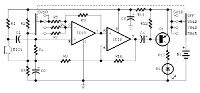
This circuit is called the detector noise environment, and also indicates by means of a flashing LED when exceeding the limit specified in the environmental noise, chosen from three fixed levels. This circuit uses two operational amplifiers, in the first position SW1 circuit is not connected, positions 2, 3 and 4 define the input sensitivity threshold to 85, 70 and 50 dB, respectively.

Environmental Noise Ratio Detector Circuit Diagram

Environmental Noise Ratio Detector Circuit Diagram


Parts List

R1 = 10K
R3 R2 = 22K
R4 = 100K
R5, R9, R10 = 56K
R6 = 5K6
R7 = 560R
R8 = 2K2
R11 = 1K
R12 = 33K
R13 = 330R
C1 = 100nF
C2 = 10μF 25V
CAP 470UF 25V C3 =
C4 = 47μF 25V
D1 = LED red
IC1 = LM358
Q1 = BC327
MIC1 = Miniature electret microphone
B1 = 9V

Dog Whistle for Ronja

Ronja is the author’s dog, a beagle-mongrel,  who seems increasingly often to need to be  called to heel either with a shout or with a  whistle. And so the idea came about for an  electronic dog whistle that could produce  two alternating high-frequency tones. A  design like this has several advantages over  conventional whistles or calling.
 
Circuit diagram :
Dog Whistle for-Ronja-Circuit-Diagram
Dog Whistle for Ronja Circuit Diagram
 
  • You can continue to carry on a conversation with your friends without having to  stop to whistle or call to your dog.
  • Using high frequencies means that  the whistle sound is barely audible to  (especially older) humans and so is less  annoying to other people than conventional whistles or calls. As is well known,  dogs have rather better hearing than  we do and can hear frequencies of up to  40 kHz.
  • The two alternating pitches mean that the  dog can more easily distinguish it from  other whistles.
 
The dog whistle is constructed from two  standard 555 timer ICs (or a single 556 IC),  both wired as astable multivibrators. The  first 555 oscillates at around 1.5 Hz and modulates the frequency of the second, which thus  switches between two different frequencies  every 0.7 seconds or so. The output of the second 555 is connected to a piezo sounder. If the  volume from the sounder used is insufficient, a small transistor amplifier can be added  between it and the output of the second 555. The circuit draws current only when activated by pressing S1. An optional green  LED indicates that the circuit is functioning.  When S2 is pressed the output frequencies  are reduced, making them more audible to  human ears for test purposes.
 
R1, R2 and C1 set the frequency of astable  multivibrator IC1. Diode D1 ensures that the  output is a symmetrical squarewave, by making C1 charge only via R1 and discharge only  via R2. Turning to IC2, where there is no diode in the  circuit, capacitor C2 is charged via R3 and R4  and discharged only via R4. With C2 = 22nF  the 555 oscillates at about 10 kHz; with S2  pressed, and hence C3 in parallel with C2, this  falls to about 1.8 kHz. Changing C2 to 10 nF  results in an even higher frequency (about  22 kHz), which can only be heard by dogs  and certain other animals. Setting C2 to 15 nF gives an output frequency of about 15 kHz. IC1 modulates the frequency of IC2 via R5. The green LED D2 is connected to the output  of IC1 via a series resistor and thus flashes at  the modulation frequency. The output from the piezo sounder at 10 kHz  (C2 = 22 nF) should be loud enough to verify  by ear. If desired, a more efficient piezo horn  tweeter can be used instead.
 

Author : Stefan Hoffmann

Simple Solar Battery Charger with LM317 Circuit Diagram

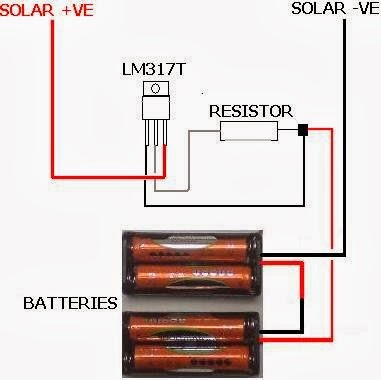
Simple Solar Battery Charger with LM317 Circuit Diagram. This is a solar panel battery charger schematic for AA and AAA rechargeable batteries. A small solar panel would be very good as a source of voltage charger. Building a solar AA battery charger only requires a few components and a simple construction. Solar panels should be well adapted to the battery to be charged or the battery may be overcharged. 

If you want to charge batteries with different capacities, then you need to change the solar panels. Since this is a simple solar battery charger that does not automatically turn off when the battery is full. So we need to maintain the charging current is low enough that will not damage the battery even when they are fully charged. An LM317T voltage regulator chip that can be used with a suitable resistor to regulate current. See solar AA battery charger 

 Solar Battery Charger with LM317 Circuit Diagram

 Solar Battery Charger with LM317 Circuit Diagram


PIC Controlled Relay Driver

This circuit is a relay driver that is based on a PIC16F84A microcontroller. The board includes four relays so this lets us to control four distinct electrical devices. The controlled device may be a heater, a lamp, a computer or a motor. To use this board in the industrial area, the supply part is designed more attentively. To minimize the effects of the ac line noises, a 1:1 line filter transformer is used.

PIC-Controlled-Relay Driver Final
The transformer is a 220V to 12V, 50Hz and 3.6VA PCB type transformer. The model seen in the photo is HRDiemen E3814056. Since it is encapsulated, the transformer is isolated from the external effects. A 250V 400mA glass fuse is used to protect the circuit from damage due to excessive current. A high power device which is connected to the same line may form unwanted high amplitude signals while turning on and off. To bypass this signal effects, a variable resistor (varistor) which has a 20mm diameter is paralelly connected to the input.
 Controller-Schematic Circuit

Another protective component on the AC line is the line filter. It minimizes the noise of the line too. The connection type determines the common or differential mode filtering. The last components in the filtering part are the unpolarized 100nF 630V capacitors. When the frequency increases, the capacitive reactance (Xc) of the capacitor decreases so it has a important role in reducing the high frequency noise effects. To increase the performance, one is connected to the input and the other one is connected to the output of the filtering part.

Supply-Schematic circuit

After the filtering part, a 1A bridge diode is connected to make a full wave rectification. A 2200 uF capacitor then stabilizes the rectified signal. The PIC controller schematic is given in the project file. It contains PIC16F84A microcontroller, NPN transistors, and SPDT type relays. When a relay is energised, it draws about 40mA. As it is seen on the schematic, the relays are connected to the RB0-RB3 pins of the PIC via BC141 transistors. When the transistor gets cut off, a reverse EMF may occur and the transistor may be defected. To overcome this unwanted situation, 1N4007 diodes are connected between the supply and the transistor collectors. There are a few number of resistors in the circuit. They are all radially mounted. Example C and HEX code files are included in the project file. It energizes the next relay after every five seconds.

The components are listed below.
1 x PIC16F84A Microcontroller
1 x 220V/12V 3.6VA (or 3.2VA) PCB Type Transformer (EI 38/13.6)
1 x Line Filter (2x10mH 1:1 Transformer)
4 x 12V Relay (SPDT Type)
4 x BC141 NPN Transistor
5 x 2 Terminal PCB Terminal Block
4 x 1N4007 Diode
1 x 250V Varistor (20mm Diameter)
1 x PCB Fuse Holder
1 x 400mA Fuse
2 x 100nF/630V Unpolarized Capacitor
1 x 220uF/25V Electrolytic Capacitor
1 x 47uF/16V Electrolytic Capacitor
1 x 10uF/16V Electrolytic Capacitor
2 x 330nF/63V Unpolarized Capacitor
1 x 100nF/63V Unpolarized Capacitor
1 x 4MHz Crystal Oscillator
2 x 22pF Capacitor
1 x 18 Pin 2 Way IC Socket
4 x 820 Ohm 1/4W Resistor
1 x 1K 1/4W Resistor
1 x 4.7K 1/4W Resistor
1 x 7805 Voltage Regulator (TO220)
1 x 7812 Voltage Regulator (TO220)
1 x 1A Bridge Diode


http://www.ecircuitslab.com

How to Build 1 2 30V 1 5A Variable Regulated Power supply Circuit


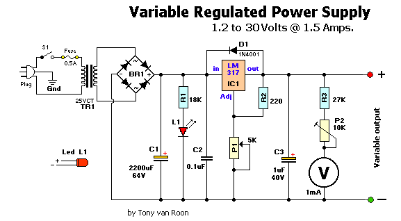
How to Build 1.2-30V/1.5A Variable Regulated Power supply, This is simple 1.2-30V/1.5A variable regulated power supply circuit diagram The 110V-AC coming from the powercord is fed to the transformer TR1 via the on-off switch and the 500mA fuse. The 30vac output (approximately) from the transformer is presented to the BR1, the bridge-rectifier, and here rectified from AC (Alternating Current) to DC (Direct Current). If you dont want to spend the money for a Bridge Rectifier, you can easily use four general purpose 1N4004 diodes. The pulsating DC output is filtered via the 2200µF capacitor (to make it more manageable for the regulator) and fed to IN-put of the adjustable LM317 regulator (IC1). The output of this regulator is your adjustable voltage of 1.2 to 30volts varied via the Adj pin and the 5K potmeter P1. The large value of C1 makes for a good, low ripple output voltage.

 1.2-30V/1.5A Variable Regulated Power supply Circuit Diagram

1.2-30V/1.5A Variable Regulated Power supply Circuit


Why exactly 1.2V and not 0-volt? Very basic, the job of the regulator is two-fold; first, it compares the output voltage to an internal reference and controls the output voltage so that it remains constant, and second, it provides a method for adjusting the output voltage to the level you want by using a potentriometer. Internally the regulator uses a zener diode to provide a fixed reference voltage of 1.2 volt across the external resistor R2. (This resistor is usually around 240 ohms, but 220 ohms will work fine without any problems). Because of this the voltage at the output can never decrease below 1.2 volts, but as the potentiometer (P1) increases in resistance the voltage accross it, due to current from the regulator plus current from R2, its voltage increases. This increases the output voltage.

D1 is a general purpose 1N4001 diode, used as a feedback blocker. It steers any current that might be coming from the device under power around the regulator to prevent the regulator from being damaged. Such reverse currents usually occur when devices are powered down.

The ON Led will be lit via the 18K resistor R1. The current through the led will be between 12 - 20mA @ 2V depending on the type and color Led you are using. C2 is a 0.1µF (100nF) decoupler capacitor to filter out the transient noise which can be induced into the supply by stray magnetic fields. Under normal conditions this capacitor is only required if the regulator is far away from the filter cap, but I added it anyway. C3 improves transient response. This means that while the regulator may perform perfectly at DC and at low frequencies, (regulating the voltage regardless of the load current), at higher frequencies it may be less effective. Adding this 1 µF capacitor should improve the response at those frequencies.

R3 and the trimmer pot (P2) alows you to zero your meter to a set voltage. The meter is a 30Volt type with an internal resistance of 85 ohms. I you have or obtained a meter with a different Ri (internal resistance) you will have to adjust R3 to keep the current of meter to 1mA. Just another note in regards this meter, use the reading as a guideline. The reading may or may not be off by about 0.75volts at full scale, meaning if your meter indicates 30 volts it may be in reality almost 31 volts or 29 volts. If you need a more precies voltage, then use your multimeter.


Construction:
Because of the few components you can use a small case but use whatever you have available. I used a power cord from a computer and cut the computer end off. All computer power cords are three-prong. The ground wire, which is connected to the middle pin of the power plug is connected to the chassis. The color of the ground-wire is either green or green/yellow. It is there for your protection if the 110vac accidentally comes in contact with the supply housing (case). BE CAREFUL always to disconnect the powerplug when you working inside the chassis. If you choose to use an in-line, or clip-type fuseholder be sure to isolate it with heat shrink or something to minimize accidental touching.

I use perf-board (or Vero board) as a circuit board. This stuff is widely available and comes relatively cheap. It is either made of some sort of fiber material or Phenolic or Bakelite pcb. They all work great. Some Phenolic boards come with copper tracks already on them which will make soldering the project together easier.

I mounted the LM317(T) regulator on a heatsink. If you use a metal/aluminum case you can mount it right to the metal case, insulated with the mica insulator and the nylon washer around the mounting screw. Note that the metal tab of the LM317 is connected internally to the Output pin. So it has to be insulated when mounting directly to the case. Use heat sink compound (comes in transparent or white color) on the metal tab and mica insulator to maximize proper heat transfer between LM317 and case/ or heatsink.

Drill the holes for the banana jacks, on/off switch, and LED and make the cut-out for the meter. It is best to mount everything in such a way that you are able to trouble-shoot your circuit board with ease if needed. One more note about the on-off switch S1, this switch has 110VAC power to it. After soldering, insulate the bare spots with a bit of silicon gel. Works great and prevents electrical shock through accidental touching.

If all is well, and you are finished assembling and soldering everything, check all connections. Check capacitors C1 & C3 for proper polarity (especially for C1, polarity reversal may cause explosion). Hookup a multimeter to the power supply output jacks. Set the meter for DC volts. Switch on S1 (led will light, no smoke or sparks?) and watch the meter movement. Adjust the potentiometer until it reads on your multimeter 15Volts. Adjust trimpot P2 until the meter also reads 15volts. When done, note any discrepancies between your multimeter and the power supply meter at full scale (max output). Maybe there is none, maybe there is a little, but you will be aware of it. Good luck and have fun building!


Parts List

BR1 = Bridge Rectifier, 100V - 3A       C1 = 2200 µF, 63V
IC1 = LM317, adjustable regulator       C2 = 0.1 µF
  V = Meter, 30V, Ri = 85 ohm           C3 = 1µF, 40V
TR1 = Transformer, 25V, 2A            Plug = 3-wire plug & cord
 R1 = 18K, 5%                           S1 = On-Off toggle switch
 R2 = 220 ohm, 5%                       D1 = 1N4001
 R3 = 27K, 5%                         Fuse = 110V, 500mA, slow-blow
 P1 = 5K, potentiometer               FuseHolder, wire, solder, case, knob for P1
 P2 = 10K, 10-turn trim-pot           Red & Black Banana Jacks

Notes:  
This is a simple, but low-ripple powersupply, and an excellent project if youre starting out in electronics. It will suit your needs for most of your bench testing and prototype applications. The output is adjustable from 1.2 volts to about 30 volts. Maximum current is about 1.5 amps which is also sufficient for most of your tinkering. It is relatively easy to build and can be pretty cheap if you have some or all the required parts. A printed circuit board is not included and Im not planning on adding one since the whole thing can easily be build on perferated or vero board. Or buy one of Radio Shack/Tandys experimentors boards (#276-150). Suit yourself. The meter and the transformer are the money suckers, but if you can scrounge them up from somewhere it will reduce the cost significantly. BR1 is a full-wave bridge rectifier. The two ~ denotes AC and are connected to the 25vac output coming from the transformer. IC1 is a 3-pin, TO-220 model. Be sure to put a cooling rib on IC1, at its max 1.5 A current it quickly becomes very hot..

All the parts can be obtained from your local Radio Shack or Tandy store. The physical size of the power supply case depends largely on the size of the meter & transformer. But almost anything will do. Go wild.


Sourced By  Tony  van roon

Power On Indicator

Some types of electronic equipment do  not provide any indication that they are  actually on when they are switched on.  This situation can occur when the back-light of a display is switched off. In addition, the otherwise mandatory mains  power  indicator  is  not  required  with  equipment  that  consumes  less  than  10 watts. As a result, you can easily forget  to switch off such equipment. If you want  to know whether equipment is still drawing power from the mains, or if you want  to have an indication that the equipment  is switched on without having to modify the equipment, this circuit provides a solution. 

image

One way to detect AC power current and  generate a reasonably constant voltage  independent of the load is to connect a  string of diodes wired in reverse parallel in series with one of the AC supply  leads. Here we selected diodes rated  at 6 A that can handle a non-repetitive  peak current of 200 A. The peak current  rating is important in connection with  switch-on  currents.  An  advantage  of  the selected diodes is that their voltage  drop increases at high currents (to 1.2 V  at 6 A). This means that you can roughly  estimate the power consumption from  the brightness of the LED (at very low  power levels). The voltage across the diodes serves as  the supply voltage for the LED driver. To  increase the sensitivity of the circuit, a  cascade circuit (voltage doubler) consisting of C1, D7, D8 and C2 is used to double  the voltage from D1–D6. Another benefit  of this arrangement is that both halve- waves of the AC current are used. We use  Schottky diodes in the cascade circuit to  minimise the voltage losses.
Circuit diagram :
Power On Indicator-Circuit-Diagram
Power On Indicator Circuit Diagram
 
The LED driver is designed to operate the LED  in blinking mode. This increases the amount  of current that can flow though the LED when  it is on, so the brightness is adequate even  with small loads. We chose a duty cycle of pproximately 5 seconds off and 0.5 second  on. If we assume a current of 2 mA for good  brightness with a low-current LED and we can  tolerate a 1-V drop in the supply voltage, the  smoothing capacitor (C2) must have a value of  1000 µF. We use an astable multivibrator built around two transistors to implement a  high-efficiency LED flasher. It is dimensioned to minimise the drive current of  the transistors. The average current consumption is approximately 0.5 mA with a  supply voltage of 3 V (2.7 mA when the  LED is on; 0.2 mA when it is off). C4 and  R4 determine the on time of the LED (0.5  to 0.6 s, depending on the supply volt-age). The LED off time is determined by  C3 and R3 and is slightly less than 5 seconds. The theoretical value is R × C × ln2,  but the actual value differs slightly due to  the low supply voltage and the selected  component values.
 
Diodes D1-D6 do not have to be special  high-voltage diodes; the reverse volt-age is only a couple of volts here due  the reverse-parallel arrangement. This  voltage drop is negligible compared to  the value of the mains voltage. The only  thing you have to pay attention to is the  maximum load. Diodes with a higher  current rating must be used above 1 kW.  In addition, the diodes may require cool-ing at such high power levels.  Measurements on D1–D6 indicate that  the voltage drop across each diode is  approximately 0.4 V at a current of 1 mA.  Our aim was to have the circuit give a  reasonable indication at current levels  of 1 mA and higher, and we succeeded  nicely. However, it is essential to use a  good low-current LED.
 
Caution: the entire circuit is at AC power potential. Never work on the circuit with the mains cable plugged in. The  best enclosure for the circuit is a small,  translucent box with the same colour as  the LED. Use reliable strain reliefs for the  mains cables entering and leaving the  box (connected to a junction box, for  example). The LED insulation does not  meet the requirements of any defined insulation class, so it must be fitted such that it  cannot be touched, which means it cannot  protrude from the enclosure. 


http://www.ecircuitslab.com

Phonon Preamplifier Circuits Diagram

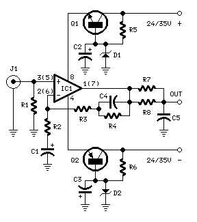
In recent years, following CDs introduction, vinyl recordings are almost disappeared. Nevertheless, a phonon preamplifier is still useful for listening old vinyl discs from a well preserved collection. This simple but efficient circuit devised for cheap moving-magnet cartridges, can be used in connection with the audio power amplifiers shown in these webpages, featuring low noise, good RIAA frequency response curve, low distortion and good high frequency transients behavior due to passive equalization in the 1 to 20KHz range. Transistors and associated components provide ±18V supply to the op-amp, improving headroom and maximum output voltage.

Phono Preamplifier Circuits Diagram
 Notes:
  • R2, R3, R4, R7, R8, C4 & C5 should be low tolerance types.
  • Schematic shows left channel and power supply.
  • For stereo operation R1, R2, R3, R4, R7, R8; J1; C1, C4 & C5 must be doubled.
  • Numbers in parentheses show IC1 right channel pin connections.

Technical data:

Sensitivity @ 1KHz: 2.5mV RMS input for 200mV RMS output
Max. input voltage @ 1KHz:120mV RMS
Max. input voltage @ 10KHz:141mV RMS
Max. input voltage @ 20KHz:127mV RMS
Frequency response @ 1V RMS output: 100Hz to 20KHz ±0.5dB; -0.75dB @ 30Hz
Total harmonic distortion @ 1KHz and 6V RMS output: 0.006%
Total harmonic distortion @10KHz and 1V RMS output: 0.02%

Parts:

R1_________47K   1/4W Resistor
R2________100R   1/4W Resistor
R3__________6K8  1/4W Resistor
R4_________68K   1/4W Resistor
R5,R6_______2K7  1/4W Resistor
R7__________2K2  1/4W Resistor
R8_________39K   1/4W Resistor
 
C1-C3_____100µF  25V Electrolytic Capacitors
C4,C5______47nF  63V Polyester Capacitors 5% tolerance
 
D1,D2__BZX79C18  18V 500mW Zener Diodes
 
IC1_______LM833  Low noise Dual Op-amp
 
Q1________BC337  45V 800mA NPN Transistor
Q2________BC327  45V 800mA PNP Transistor
 
J1__________RCA  audio input socket


High Performance 12V 20W Stereo Amplifier

High-Performance 12V 20W Stereo Amplifier. Amplifiers which run from 12V DC generally don’t put out much power and they are usually not hifi as well. But this little stereo amplifier ticks the power and low distortion boxes. With a 14.4V supply, it will deliver 20 watts per channel into 4-ohm loads at clipping while harmonic distortion at lower power levels is typically less than 0.03%. This is an ideal project for anyone wanting a compact stereo amplifier that can run from a 12V battery. It could be just the ticket for buskers who want a small but gutsy amplifier which will run from an SLA battery or it could used anywhere that 12V DC is available – in cars, recreational vehicles, remote houses with 12V DC power or where ever.

12v-20watt-stereo-amplifier-
20W Stereo Audio Amplifier

Because it runs from DC, it will be an ideal beginner’s or schoolie’s project, with no 240VAC power supply to worry about. You can run it from a 12V battery or a DC plugpack. But while it may be compact and simple to build, there is no need to apologise for “just average” performance. In listening tests from a range of compact discs, we were very impressed with the sound quality. Long-time readers might recall that we presented a similar 12V power amplifier design back in May 2001. It was a similar configuration to this one but it is now completely over-shadowed by the much lower distortion and greatly improved signal-to-noise ratio of this new design. In fact, let’s be honest: the previous unit is not a patch on this new design. It used two TDA1519A ICs which resulted in distortion figures above 1% virtually across the board and a signal-to-noise ratio of only -69dB unweighted.
.
20W Stereo Amplifier Circuit 20W Stereo Amplifier Circuit

However, by using the TDA­7377 power amplifier IC and making some other improvements, the THD (total harmonic distortion) of the new design is about 50 times better than the older unit (see performance graphs for details). The bottom line is that the THD under typical conditions is around just 0.03% or less. It is also able to deliver more output power due to the improved output transistors in the new power amplifier IC. In addition, its idle power consumption is low – not much more than 1W. As a result, if you don’t push it too hard it will run cool and won’t drain the battery too quickly. And because the IC has self-protection circuitry, it’s just about indestructible. It will self-limit or shut down if it overheats and the outputs are deactivated if they are shorted.

Circuit diagram:
12v-20watt-stereo-amplifier-circuit-diagram12
20W Stereo Amplifier Circuit Diagram

With a 12V supply, the largest voltage swing a conventional solid-state power amplifier can generate is ±6V. This results in a meagre 4.5W RMS into 4O and 2.25W RMS into 8O, without considering losses in the output transistors. Even if the DC supply is around 14.4V (the maximum that can normally be expected from a 12V car battery), that only brings the power figures up to 6.48W and 3.24W for 4O and 8O loads respectively – still not really enough. There are three common solutions to this problem. The first is to boost the supply voltage using a switchmode DC converter. This greatly increases the cost and complexity of the amplifier but it is one way of getting a lot of power from a 12V supply. However, we wanted to keep this project simple and that rules out this technique.

Parts layout:
Parts layout 20w-stereo-amplifier


There are variations on the boosting method, such as the class H architecture used in the TDA1562Q IC featured in the Portapal PA Amplifier (SILICON CHIP, February 2003). It is able to achieve 40W/channel but with >0.1% THD. In that case, the amplifier output itself provides the switching for a charge pump. The second method is to lower the speaker impedance. Some car speakers have an impedance as low as 2O, which allows twice as much power to be delivered at the same supply voltage. However, we don’t want to restrict this amplifier to 2O loudspeakers.


Author: Nicholas Vinen - Copyright: Silicon Chip

Build a Toggle Touch Switch Using Two Inverter Gates

We  can make a simple touch switch using only two inverter gates, two resistors, and two capacitors. The schematic diagram of the circuit is shown in the figure below. At power up, the output (of U1A) will be high, and the inverting output will be low because U1A gate will be triggered to ground level by C2. After triggered, the low level of U1A input is maintained by U1B output via R2.

If we touch the pad at this condition, where the output is high, then the U1A input will go high because we “short” the voltage of C1 to the input pin, and the low level previously caused by low level of U1B output voltage connected via R2 can’t be maintained because our skin resistance is much lower than 10M.

After U1A input goes high then U1A output will go low, and now U1B will go high to maintain high voltage level of U1A via R2, so we can release our finger without loosing the last state. Touching the pad again after we release our previous touching will toggle the output as the condition is reversed.

After we touch the pad, we have to release before 1 second (R2C2 time constant) elapsed. If we touch the pad longer than R2C2 time constant then  the output will oscillate (about 1 Hz).


Save Your Ears A Noise Meter

‘Hello… HELLO! Are you deaf? Do you have disco ears?’ If people ask you this and you’re still well below 80 , you may be suffering from hearing loss, which can come from (prolonged) listening to very loud music. You won’t notice how bad it is until it’s too late, and after that you won’t be able to hear your favorite music the way it really is – so an expensive sound system is no longer a sound investment. To avoid all this, use the i-trixx sound meter to save your ears (and your neighbors ears!).
With just a handful of components, you can build a simple but effective sound level meter for your sound system. This sort of circuit is also called a VU meter. The abbreviation ‘VU’ stands for ‘volume unit’, which is used to express the average value of a music signal over a short time. The VU meter described here is what is called a ‘passive’ type. This means it does not need a separate power supply, since the power is provided by the input signal. This makes it easy to use: just connect it to the loudspeaker terminals (the polarity doesn’t matter) and you’re all set.
The more LEDs that light up while the music is playing, the more you should be asking yourself how well you are treating your ears (and your neighbours’ ears). Of course, this isn’t an accurately calibrated meter. The circuit design is too simple (and too inexpensive) for that. However, you can have a non-disco type (or your neighbors) tell you when the music is really too loud, and the maximum number of LED lit up at that time can serve you as a good reference for the maximum tolerable sound level.
Although this is a passive VU meter, it contains active components in the form of two transistors and six FETs. Seven LEDs light up in steps to show how much power is being pumped into the loudspeaker. The steps correspond to the power levels shown in the schematic for a sine-wave signal into an 8-ohm load. LED D1 lights up fi rst at low loudspeaker voltages. As the music power increases, the following LEDs (D2, D3, and so on) light up as well. The LEDs thus dance to the rhythm of the music (especially the bass notes).
Circuit diagram:
noise meter circuit diagram Noise Meter Circuit Diagram
This circuit can easily be assembled on a small piece of prototyping board. Use low-current types for the LEDs. They have a low forward voltage and are fairly bright at current levels as low as 1 mA. Connect the VU meter to the loudspeaker you want to monitor. If LED D2 never lights up (it remains dark even when LED D3 lights up), reverse the polarity of diode D8 (we have more to say about this later on). In addition, bear in mind that the sound from the speaker will have to be fairly loud before the LEDs will start lighting up.
If you want to know more about the technical details this VU meter, keep on reading. Each LED is driven by its own current source so it will not be overloaded with too much current when the input voltage increases. The current sources also ensure that the final amplifier is not loaded any more than necessary. The current sources for LEDs D1–D6 are formed by FET circuits. A FET can be made to supply a fixed current by simply connecting a resistor to the source lead (resistors R1–R6 in this case). With a resistance of 1 kΩ, the current is theoretically limited to 1 mA. However, in practice FETs have a especially broad tolerance range. The actual current level with our prototype ranged from 0.65 mA to 0.98 mA.
To ensure that each LED only lights up starting at a defined voltage, a Zener diode (D8–D13) is connected in series with each LED starting with D2. The Zener voltage must be approximately 3 V less than the voltage necessary for the indicated power level. The 3-V offset is a consequence of the voltage losses resulting from the LED, the FET, the rectifier, and the over voltage protection. The over voltage protection is combined with the current source for LED D7. One problem with using FETs as current sources is that the maximum rated drain–source voltage of the types used here is only 30 V.
If you want to use the circuit with an especially powerful fi nal amplifier, a maximum input level of slightly more than 30 V is much too low. We thus decided to double the limit. This job is handled by T7 and T8. If the amplitude of the applied signal is less than 30 V, T8 buffers the rectified voltage on C1. This means that when only the first LED is lit, the additional voltage drop of the over voltage protection circuit is primarily determined by the base–emitter voltage of T8. The maximum worst-case voltage drop across R8 is 0.7 V when all the LEDs are on, but it has increasingly less effect as the input voltage rises.
R8 is necessary so the base voltage can be regulated. R7 is fitted in series with LED D7 and Zener diode D13, and the voltage drop across R7 is used to cause transistor T7 to conduct. This voltage may be around 0.3 V at very low current levels, but with a current of a few mili-amperes it can be assumed to be 0.6 V. Transistor T7 starts conducting if the input voltage rises above the threshold voltage of D7 and D13, and this reduces the voltage on the base of T8. This negative feedback stabilizes the supply voltage for the LEDs at a level of around 30 V. With a value of 390 Ω for R7, the current through LED D7 will be slightly more than 1 mA.
This has been done intentionally so D7 will be a bit brighter than the other LEDs when the signal level is above 30 V. When the voltage is higher than 30 V, the circuit draws additional current due to the voltage drop across R8. The AC voltage on the loudspeaker terminals is half-wave rectifi ed by diode D14. This standard diode can handle 1 A at 400 V. The peak current level can be considerably higher, but don’t forget that the current still has to be provided by the fi nal amplifier.
Resistor R9 is included in series with the input to keep the additional load on the fi nal amplifi er within safe bounds and limit the interference or distortion that may result from this load. The peak current can never exceed 1.5 A (the charging current of C1), even when the circuit is connected directly to an AC voltage with an amplitude of 60 V. C1 also determines how long the LEDs stay lit. This brings us to an important aspect of the circuit, which you may wish to experiment with in combination with the current through the LEDs.
An important consideration in the circuit design is to keep the load on the fi nal amplifi er to a minimum. However, the combination of R9 and C1 causes an averaging of the complex music signal. The peak signal levels in the music are higher (or even much higher) than the average value. Tests made under actual conditions show that the applied peak power can easily be a factor of 2 to 4 greater than what is indicated by this VU meter. This amounts to 240 W or more with an 8-Ω loudspeaker.
You can reduce the value of C1 to make the circuit respond more quickly (and thus more accurately) to peak signal levels. Now a few comments on D8. You may receive a stabistor (for example, from the Philips BZV86 series or the like) for D8. Unlike a Zener diode, a stabistor must be connected in the forward-biased direction. A stabistor actually consists of a set of PN junctions in series (or ordinary forward-biased diodes). Check this carefully: if D2 does not light up when D8 is fi tted as a normal Zener diode, then D8 quite likely a stabistor, so you should fi t it the other way round.

Surf Sound Synthesizer

Many people who live close to the ocean have the benefit of being lulled to sleep by the sound of the surf. This circuit may provide a similar benefit to all those poor unfortunates who don’t live near the seaside but who do have the small consolation that they don’t have to worry about rust and corrosion in a salty atmosphere. The circuit consists of four unsynchronised oscillators which are mixed together to modulate a white noise source to simulate the more or less random nature of surf sounds. You won’t hear the waves crashing but the ebb and flow of the white noise will help mask other noises which would otherwise disturb your sleep.

Surf Sound Synthesizer circuit diagram
The four oscillators are based on four op amps in a TL074 or TL084 quad op amp package (IC1). IC1a, IC1b, IC1c & IC1d are configured as Schmitt trigger oscillators with their operating frequencies defined by the resistor connected between their outputs (pins 1, 7, 8 & 14) and the respective inverting inputs (pins 2, 6, 9 & 13), as well as the electrolytic capacitors connected between these latter pins and 0V. The result is a triangle waveform at each of the respective inverting inputs and square waves at the same frequencies at the op amp outputs. We don’t use the square outputs but instead feed the four triangle waveforms to op amp IC2a which is connected as a mixer. Its output is used to drive and modulate a noise source based on NPN transistor Q1. This is operated with reverse bias across its base-emitter junction and the controlled reverse current is very noisy.

By varying the amount of reverse bias, we vary the amount of white noise produced. Since the amount of noise produced by the transistor varies markedly between types, the gain of IC2a can be varied over a wide range to produce the optimum output voltage to drive Q1. From there, the noise signal from the emitter of Q1 is fed via a 47nF capacitor to op amp IC2b which can also have its gain varied over a wide range to drive IC3, an LM386 power amplifier which drives the loudspeaker. In use, first adjust trimpot VR2 to set the volume level from the loudspeaker, then adjust trimpot VR1 to get the best range of white noise which simulates the surf sounds. Sleep well.

Rolling Shutter Motor Control

An electrically operated rolling shutter usually has a standard control panel with a three-position switch: up, down and stop. If you would like to automate the opening and closing with a time controlled switch, a few additional wires will have to be connected. Typically, the controls are implemented as indicated in the schematic ‘Normal Situation’. If this is indeed the case, then you can see in ‘New Situation’ how the shutter can be automated with a timer. There is only one method to determine the actual schematic of your control circuit, and that is to open the control box and using an ohmmeter, pencil and paper to check out and draw the circuit. Make sure you turn the power off first though! Connect a 230-V relay (with both the contacts and the coil rated 230 VAC) to the timer.

Rolling_Shutter_Control2 Circuit Diagram 
The changeover switch between automatic and manual control needs to be rated 230 VAC as well and may not be a hazard for the user. The relay and switch are preferably fitted in a plastic mains adapter enclosure with built-in plug, which is plugged into the timer. It is a good idea to check first if this will actually fit. Because of the manual/automatic-switch, the operation is completely fail-safe and misunderstandings are out of the question. The switch prevents the issue of conflicting commands (with disastrous consequences) when, for example, the shutter is being automatically raised and manually lowered at the same time.

Rolling_Shutter_Control Circuit Diagram


Source: http://www.ecircuitslab.com/2011/05/rolling-shutter-motor-control.html

30W Power Audio Amplifier Circuit Diagram

TIP141 si a npn silicon power darling tons designed for complementary use with TIP145, TIP146 and TP147. Can stand up to 125 W at 25°C Case Temperature, 10 A Continuous Collector Current and has a minimum hFE of 1000 at 4 V, 5 A. This home audio amplifier can output 30W with a +- 32V symmetric power supply. If you want a stereo power amplifier please check out the other schematics.


R1=1Kohm R16-17=270ohm D1=9.1V 0.4W zener
R2=47Kohm R18=22ohm 1W D2-3=1N4148
R3=1.5Kohm R19=NC Q1-2=BC550C
R4-5=10Kohm R20-21=0.39ohm 4W Q3=MPSA56
R6=5.6Kohm TR1=250ohm trimmer Q4=BC547B
R7=10ohm C1=470nF 100V MKT Q5=BC212
R8=47Kohm C2=1nF 100V MKT Q6=BC183
R9=560ohm C3=68pF ceramic Q7-8=MPSAO6
R10-11=8.2Kohm C4-8=22nF 100V MKT Q9=TIP141
R12-15=120ohm C5-6-7=100nF 100V MKT Q10=TIP146
R13=680ohm C9=47uF 25V F1-2=1.6AT FUSE
R14=330ohm C10-11=220uF 63V All the resistors is 1/4W 1% except quote differently

30W power amplifier circuit diagram

30W power amplifier circuit diagram

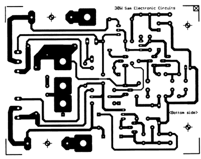
30 Watt audio amplifier PCB

30 Watt audio amplifier PCB


Simple Park Assist Circuit Diagram

Build a  Park Assist Circuit Diagram. This is a Simple Park Assist Circuit Diagram. This Park Assist circuit was designed as an aid in parking the car near the garage wall when backing up. LED D7 illuminates when bumper-wall distance is about 20 cm., D7+D6 illuminate at about 10 cm. and D7+D6+D5 at about 6 cm. In this manner you are alerted when approaching too close to the wall. 

All distances mentioned before can vary, depending on infra-red transmitting and receiving LEDs used and are mostly affected by the color of the reflecting surface. Black surfaces lower greatly the device sensitivity. Obviously, you can use this circuit in other applications like liquids level detection, proximity devices etc. 

 Simple Park Assist Circuit Diagram


Simple Park Assist Circuit Diagram

Monitor voltage and 5VDC and 12VDC Circuit Diagram

This circuit is a voltage monitor which operates on fixed testes ± 5 VDC and ± 12 VDC, and is easily constructed as shown in Fig. It is considerably simpler than the normal display using comparators and AND gates. The circuit is not intended to indicate the level of entries. If one of the testes fail, for example, -5 V line fails, the transistor Q3 remains on but the base-emitter junction of T2 is not, so that this transistor is cut off. When this happens, there is no current through D, which then turns off.

Monitor voltage + and - 5VDC + and - 12VDC Circuit Diagram

Monitor voltage + and - 5VDC + and - 12VDC Circuit Diagram

Simple USB Standby Killer

When turning a computer on and off, various peripherals (such as printers, screen, scanner, etc.) often have to be turned on and off as well. By using the 5-V supply voltage from the USB interface on the PC, all these peripherals can easily be switched on and off at the same time as the PC. This principle can also be used with other appliances that have a USB interface (such as modern TVs and radios). 

USB Standby Killer Circuit Diagram :
USB-Standby-Killer-Circuit Diagram

This so-called ‘USB-standby-killer’ can be realised with just 5 components.
The USB output voltage provides for the activation of the triac-opto driver (MOC3043) which has zero-crossing detection. This, in turn, drives the TRIAC, type BT126. 

The circuit shown is used by the author for switching loads with a total power of about 150 W and is protected with a 1-A fuse. The circuit can easily handle much larger loads however. In that case and/or when using a very inductive load a so-called snub-ber network is required across the triac. The value of the fuse will also need to be changed as appropriate. 

The circuit can easily be built into a mains multi-way power board. Make sure you have good isolation between the USB and mains sections (refer to the Electrical Safety page published regularly in this magazine). 


Source by : http://www.ecircuitslab.com/2012/08/usb-standby-killer.html

Mains Voltage Monitor

Many electronics hobbyists will have experienced the following: you try to finish a project late at night, and the mains supply fails. Whether that is caused by the electricity board or your carelessness isn’t really important. In any case, at such times you may find yourself without a torch or with flat batteries. There is no need to panic, as this circuit provides an emergency light. When the mains fails, the mains voltage monitor turns on five super bright LEDs, which are fed from a 9 V battery (NiCd or NiMH) or 7 AA cells. A buzzer has also been included, which should wake you from your sleep when the mains fails.

You obviously wouldn’t want to oversleep because your clock radio had reset, would you? When the mains voltage is present, the battery is charged via relay Re1, diode D8 and resistor R10. D8 prevents the battery voltage from powering the relay, and makes sure that the relay switches off when the mains voltage disappears. R10 is chosen such that the charging current of the battery is only a few milliamps. This current is small enough to prevent over-charging the battery. D6 acts as a mains indicator. When the relay turns off, IC1 receives power from the battery. The JK flip-flops are set via R12 and C4.

Circuit diagram:
mains-voltage-monitor-circuit diagram
Mains Voltage Monitor Circuit Diagram

This causes T1 and T2 to conduct, which turns on D1-D5 and the buzzer. When the push button is pressed, a clock pulse appears on the CLK input of flip-flop IC1b. The output then toggles and the LEDs turn off. At the same time IC1a is reset, which silences the buzzer. If you press the button again, the LEDs will turn on since IC1b receives another clock pulse. The buzzer remains off because IC1a stays in its reset state. R11, R3 and C3 help to debounce the push button signal. In this way the circuit can also be used as a torch, especially if a separate mains adapter is used as the power supply.

As soon as the mains voltage is restored, the relay turns on, the LEDs turn off and the battery starts charging. The function of R13 is to discharge C4, preparing the circuit for the next mishap. If mains failures are a regular occurrence, we recommend that you connect pairs of LEDs in series. The series resistors should then have a value of 100 ?. This reduces the current consumption and therefore extends the battery life. This proves very useful when the battery hasn’t recharged fully after the last time. In any case, you should buy the brightest LEDs you can get hold of. If the LEDs you use have a maximum current of 20 mA, you should double the value of the series resistors! You could also consider using white LEDs.


Author: Goswin Visschers - Copyright: Elektor July-August 2004

Car Battery 12v Charger

The usual chargers of battery automotive, are simple and cheap appliances that charge continuously the battery, with a rythm of few amperes, for the time where the appliance is ON. If the holder do not close in time the charger, the battery will overcharge and her electrolytic faculty are lost with evaporation or likely exists destruction of her elements. The charger of circuit exceeds these faults. It checks electronic the situation of charge of battery and it has circuit of control with retroaction, that forces the battery charge with biggest rythm until charge completely.
Circuit diagram:
Car_baterry_charger Circuit Diagram
Car Battery 12v Charger Circuit Diaram
When charge completely, it turns on one RED led (LD2). The charger has been drawn in order to charge batteries of 12V, ONLY. What should watch it from what it manufactures the circuit, they are the cables that connect the transformer with the circuit and in the continuity the battery, should they are big cross-section, so that heat when it passes from in them the current of charge and also they do not cause fall of voltage at the way of current through them.
Adjustment
After assembling of the circuit, adjust TR1 to null value, power-up and make the following adjustments :-
  1. Without connecting the battery check that the 2 LED?s are turned on.
  2. Connect a car battery to the circuit and check that LD2 is OFF and a current (normally 2A to 4A) is flowing to the battery.
  3. Adjust TR1 until LD2 turns ON and the charge current is cut.
  4. Adjust TR1 to null value and charge the battery using the hydrometer technique (if you do not have or do not know how to use a hydrometer, then use a good condition battery and charge).

Carefully adjust TR1 so that LD2 begins to turn ON and the charge current falls to a few hundred milliamps (mA). If TR1 is set correctly then in the next round of charging you will noticed LD2 begin to flicker as the battery is being charged. When battery is completely charged, LD2 turns ON completely.TR1 does not need further adjustment anymore. Q1 is connected in line with the battery and is fired by R3, R4 and LD2. The R2, C1, TR1 and D2 sense the voltage of the battery terminal and activate Q2 when the voltage of the battery terminal exceeds the value predetermined by TR1.

When an uncharged battery is connected, the terminal voltage is low. Under this circumstance, Q2 is turned OFF and Q1 is fired in each half cycle by R3, R4 and LD2. The Q1 functions as a simple rectifier and charges the battery. If the battery terminal voltage is increased above the level that had been fixed by TR1, then Q2 shifts the control of Q1 gate. This deactivates Q1 and cuts off the current supply to the battery and turns LD2 ON indicating that the charge has been completed. Q1 and bridge rectifier GR1 should be mounted on heatsinks to prevent overheating. M1 is a 5A DC ammeter to measure the charge current.

Source :users.otenet.gr

New 4 Channel Portable Audio Mixer

The target of this project was the design of a small portable mixer supplied by a 9V PP3 battery, keeping high quality performance. The mixer is formed assembling three main modules that can be varied in number and/or disposition to suit everyone needs. The three main modules are:

Input Amplifier Module: a low noise circuit equipped with a variable voltage-gain (10 - 100) preset, primarily intended as high quality microphone input, also suitable for low-level line input.

Tone Control Module: a three-band (Bass, Middle, Treble) tone control circuit providing unity-gain when its controls are set to flat frequency response. It can be inserted after one or more Input Amplifier Modules and/or after the Main Mixer Amplifiers.

Main Mixer Amplifier Module: a stereo circuit incorporating two virtual-earth mixers and showing the connection of one Main Fader and one Pan-Pot.

The image below shows a Block diagram of the entire mixer featuring four Input Amplifier Modules followed by four in-out switchable Tone Control Modules, one stereo Line input, four mono Main Faders, one stereo dual-ganged Main Fader, four Pan-Pots, a stereo Main Mixer Amplifier Module and two further Tone Control Modules switchable in and out for each channel, inserted before the main Left and Right outputs.

Obviously this layout can be rearranged at everyone wish. An astonishing feature of this design lies in the fact that a complete stereo mixer as shown below in the Block diagram draws less than 6mA current!

Block diagram:

4 channel input mixer

Input Amplifier Module
Circuit Diagram:

Parts:

R1 = 22K - 1/4W Resistor
R2 = 22K - 1/4W Resistor
R3 = 47K - 1/4W Resistor
R4 = 47K - 1/4W Resistor
R5 = 47K - 1/4W Resistor
R6 = 4K7 - 1/4W Resistor
R7 = 22K - 1/4W Resistor
R8 = 220R - 1/4W Resistor
R9 = 2K - 1/2W Trimmer Cermet (See Notes)
R10 = 470K - 1/4W Resistor
R11 = 560R - 1/4W Resistor
R12 = 100K - 1/4W Resistor
R13 = 220R - 1/4W Resistor

C1 = 470nF - 63V Polyester Capacitor
C2 = 100µF - 25V Electrolytic Capacitor
C3 = 2µ2 - 63V Electrolytic Capacitor
C4 = 2µ2 - 63V Electrolytic Capacitor
C5 = 2µ2 - 63V Electrolytic Capacitor
C6 = 47pF - 63V Ceramic Capacitor
C7 = 4µ7 - 63V Electrolytic Capacitor
C8 = 100µF - 25V Electrolytic Capacitor
Q1 = BC560C - 45V 100mA Low noise High gain PNP Transistor
Q2 = BC550C - 45V 100mA Low noise High gain NPN Transistor
IC1 = TL061 - Low current BIFET Op-Amp

Circuit Description:

The basic arrangement of this circuit is derived from the old Quad magnetic pick-up cartridge module. The circuit was rearranged to cope with microphone input and a single-rail low voltage supply. This low-noise, fully symmetrical, two-transistor head amplifier layout, allows the use of a normal FET input Op-Amp as the second gain stage, even for very sensitive microphone inputs. The voltage-gain of this amplifier can be varied by means of R9 from 10 to 100, i.e. 20 to 40dB.

Notes:
  • R9 can be a trimmer, a linear potentiometer or a fixed-value resistor at will.
  • When voltage-gain is set to 10, the amplifier can cope with 800mV peak-to-peak maximum Line levels.
  • Current drawing for one Input Amplifier Module is 600µA.
  • Frequency response is 20Hz to 20KHz - 0.5dB.
  • Total Harmonic Distortion measured with voltage-gain set to 100: 2V RMS output = <0.02%>
  • Total Harmonic Distortion measured with voltage-gain set to 10 & 33: 2V RMS output = <0.02%>
  • THD is much lower @ 1V RMS output.
  • Maximum undistorted output voltage: 2.8V RMS.

A Car Battery Monitor

A close call on the road can really focus your mind on the importance of having a battery monitor in a car. I had been enjoying a pleasant week of travelling around the countryside at a leisurely pace and taking in the beautiful scenery each day. It wasnt until the final day, with the big rush to return home, that I had to drive at night.My home is deep in the country and on the road I was travelling the closest petrol station may be 80km away. I was travelling through an area that is full of open-cut coal mines and large heavily loaded semi-trailers constantly pound the roads, travelling at quite high speeds. It was around 8pm at night and everything was very dark no street lights or house lights anywhere.

Just as I was going up a hill, the lights began to dim and the engine coughed. A large semi-trailer loomed in the rear-vision mirror as I pushed the clutch in and tried to restart. My speed was falling rapidly and my lights were blacked out - I was like a sitting duck in the middle of the road, as the semi-trailer came rapidly bearing down on me. I just managed to pull the car off the road, as the semi-trailer came screaming past, missing me by inches! After calling for assistance from the NRMA, the problem was found to be a fault in the alternator, which was failing to charge the battery. The battery voltage had been falling under the heavy load of the lights and at the worst possible time, there was not sufficient power for the lights or the motor.

After the initial shock wore off, I put on my thinking cap to come up with a PIC-based solution to the problem. What was really needed was a display and a buzzer, to get my attention should the voltage fall outside a specified range. So my design criteria was set, a series of LEDs could indicate the voltage and a buzzer would also be used to warn of problems.
Main Features:
  • Visual indication of battery voltage
  • Audible warning when voltage becomes low
  • Screw terminals for easy connection
  • Simple and easy to build
Circuit details:

The circuit is based on PIC16F819 18-pin microcontroller which has an analog-to-digital (A/D) input to monitor the battery voltage and outputs capable of driving LEDs directly, to keep the component count down. There are seven LEDs in all, giving a good range of voltage indication. The topmost LED, LED1, comes on for voltages above 14V which will occur when the battery is fully charged. LED2 indicates for voltages between 13.5V and 14V while LED3 indicates between 13V and 13.5V. Normally, one of these LEDs will be on. LED4 covers 12.5V to 13V while LED5 covers 12V to 12.5V. LED6 covers from 11.5V to 12V while LED7 comes on for voltages below 11.5V. These two LEDs are backed up by the piezo chime which beeps for voltages between 11.5V and 12V and becomes more insistent for voltages below 11.5V.

That might seem fairly conservative. After all, most cars will start with no troubles, even though the battery voltage might be a touch below 12V, wont they? Well, no. Some modern cars will happily crank the motor at voltages below 11V but their engine management will not let the motor start unless the voltage is above 11V. So dont think that a modern car will always start reliably. This little battery monitor could easily prevent a very inconvenient failure to start! So lets describe the rest of the circuit. The incoming supply is connected via diode D1 which provides protection against reverse polarity while zener diode ZD1 provides protection from spike voltages.

A standard 7805 3-terminal regulator is then used to provide a stable 5V to the microcontroller. The battery voltage is sensed via a voltage divider using 33kΩ and 100kΩ resistors. This brings the voltage down to within the 0-5V range for the A/D input of the PIC16F819. Port B (RB0 to RB7) of the microcontroller is then used to drive the various LEDs, with current limiting provided via the 330Ω resistor network. RB7, pin 13, drives a switching transistor for the piezo buzzer.

Software:
For the software, the design follows the basic template for a PIC microcontroller. Port A and its ADC (analog-to-digital converter) function are set up while port B functions as the output for the LEDs and buzzer. Once the set-up is complete, a reading will be taken at port RA2, the input for the A/D convertor. This reading is then compared with a series of values to determine the range of the voltage. This is similar to a series of "if" statements in Basic language. If the voltage is found to be within a certain range, the relevant port B pin will be turned on. If the voltage is below 12V, the buzzer will be turned on for a brief period, to signal a low battery condition. As the voltage falls below 11.5V, the frequency of the beeps will increase, to signal increased urgency.

Building it:

All the parts are mounted on a small PC board measuring 46 x 46mm (available from Futurlec). The starting point should be the IC socket for the PIC16F819, as this is easiest to mount while the board is bare. The next item can be the PC terminal block. The resistors and capacitors can then follow. Make sure the electrolytics are inserted with correct polarity.

Make sure that you do not confuse the zener (ZD1) with the diode when you are installing them; the diode is the larger package of the two.
 
Even more important, dont get the 78L05 3-terminal regulator and the 2N3906 transistor mixed up; they come in identical packages. The 78L05 will be labelled as such while the 2N3906 will be labelled "3906". And make sure you insert them the correct way around. The buzzer must also be installed with the correct polarity. The 330Ω current limiting resistors are all in a 10-pin in-line package. There are four green LEDs, two yellow and one red. They need to be installed in line and with the correct orientation.

Testing:

Before you insert the PIC16F819 microcontroller, do a voltage check. Connect a 12V source and check for the presence of 5V between pins 14 & 5 OF IC1. If 5V is not present, check the polarity of regulator REG1 and the polarity of the diode D1. If these tests are OK, insert the IC and test the unit over a range of voltage between 9V and 15V. Make sure that all LEDs come on in sequence and the piezo buzzer beeps for voltages below 12V. 

Now it is matter of installing the unit in your car. It is preferable to install the unit in a visible position for the driver. However, it should not obscure any other instruments. The unit should be connected to the cars 12V supply after the ignition switch. This will turn the unit off with the other instruments and prevent battery drain while the motor is not running.


Author :Alan Bonnard Copyright : Silicon Chip Publications Pty Ltd

Little Door Guard

If some intruder tries to open the door of your house, this circuit sounds an alarm to alert you against the attempted intrusion. The circuit (Fig. 1) uses readily available, low-cost components. For compactness, an alkaline 12V battery is used for powering the unit. Input DC supply is further regulated to a steady DC voltage of 5V by 3-pin regulator IC 7805 (IC2).


Circuit of the door guard
Fig. 1: Circuit of the door guard

Assemble the unit on a general-purpose PCB as shown in Fig. 4 and mount the same on the door as shown in Fig. 3. Now mount a piece of mirror on the door frame such that it is exactly aligned with the unit. Pin configurations of IC UM3561 and transistors 2N5777 and BC547 are shown in Fig. 2. 

UM3561 and transistors
Fig. 2: Pin configurations of UM3561 and transistors 2N5777 and BC547

Initially, when the door is closed, the infrared (IR) beam transmitted by IR LED1 is reflected (by the mirror) back to phototransistor 2N5777 (T1). The IR beam falling on phototransistor T1 reverse biases npn transistor T2 and IC1 does not get positive supply at its pin 5. As a result, no tone is produced at its output pin 3 and the loudspeaker remains silent. Resistor R1 limits the operating current for the IR LED.
When the door isopened, the absence of IR rays at phototransistor T1 forward biases npn transistor T2, which provides supply to  positiveIC1. Now 3-sirensound generator IC UM3561 (IC1) gets power via resistor R5. The output of IC1 at pin 3 is amplified by Darlington-pair transistors T3 and T4 to produce the alert tone via the loudspeaker. 

Back view of the door assembly
Fig. 3: Back view of the door assembly

Rotary switch S2 is used to select the three preprogrammed tones of IC1. IC1 produces fire engine, police and ambulance siren sounds when its pin 6 is connected to point F, P or A, respectively.

Suggested enclosure
Fig. 4: Suggested enclosure with major components layout


Author : T.K. Hareendran - Copyright : EFY