Showing posts with label supply. Show all posts

Thursday, November 20, 2014

1 3V DC to 12 2V DC Regulator Power Supply

Power supply circuit to generate output below were variations between 1.3V DC to 12.2V DC with 1A current.
In addition, the power supply circuit is also equipped with over-current protection or shield against belebih flow. Power supply circuit is very simple, but the quality is quite good, made her basiskan regulator IC LM723 is a pretty legendary.


1.3V


Description:

R2 to set the output voltage. The maximum current is determined by R3, over-current protection circuit inside the LM723 to detect the voltage on R3, if it reaches 0.65 V, the voltage output will be off her. So the current through R3 can not exceed 0.65 / R3 although output short-circuit in his.

C3 and C4 are ceramic capacitors, as much as possible directly soldered to the PCB, this is because the LM723 is prone to oscillation that is not cool.

LM723 works with 9.5V input voltage to 40 V DC and the LM723 can generate its own current of 150mA when the output voltage is not more than 6-7V under input voltage.


Specifications:

Output (value estimated):

Vmin = (R4 + R5) / (R5 * 1.3)
Vmax = (7.15 / R5) * (R4 + R5)
Imax = 0.65/R3
Max. Power on R3: 0.42/R3


Min. DC Input Voltage (pin 12 to pin 7): Vmax + 5

Component List:

B1 40V/2.5A
C1 2200uF (3300uF even better)
C2 4.7uF
C3 100nF
C4 1NF
C5 330nF
C6 100uF
Green LED D1
D2 1N4003
F1 0.2A F
F2 2A M
IC1 LM723 (in a DIL14 plastic package)
R1 1k
R2 Pot. 5k
R3 0.56R/2W
R4 3.3k
R5 4.7k
S1 250V/1A
T1 2N3055 on a heatsink 5K / W
TR1 220V/17V/1.5

Sunday, November 16, 2014

Power supply using tube Z2C

Power supply using tube Z2C are designed specifically to provide power supply voltage to the EL-34 tube amplifier push-pull in the previous article. Power supply with Z2C tube to tube power amplifier is made with a tube rectifier Z2C.
Just as the power supply for power amplifier tubes previously, the power supply is also using a filter with 3 levels of electrolytic capacitors. The circuit power supply with tube rectifier can deliver Z2C +210 VDC output voltage.
Power
Z2C on the rectifier tube in power supply with tube above requires a supply voltage for the filaments taken from the other side of the transformer secondary. Z2C tube power supply with a power supply that is used as a substitute DAPT power supply for power amplifier tubes with a diode

Friday, November 14, 2014

STABILIZED POWER SUPPLY 3 30 V 2 5 A

This is a versatile power supply that will solve most of the supply problems arising in the everyday work of any electronics workshop. It covers a wide range of voltages being continuously variable from 30 V down to 3 V. The output current is 2.5 A maximum, more than enough for most applications. The circuit is completely stabilised even at the extremes of its output range and is fully protected against short-circuits and overloading.

Circuit Diagram


Working

The power supply is using a well known and quite popular VOLTAGE STABILIZER IC the LM 723. The IC can be adjusted for output voltages that vary continuously between 2 and 37 VDC and has a current rating of 150 mA which is of course too low for any serious use. In order to increase the current handling capacity of the circuit the output of the IC is used to drive a darlington pair formed by two power transistors the BD 135 and the 2N 3055. The use of the transistors to increase the maximum current output limits the range of output voltages somewhat and this is why the circuit has been designed to operate from 3 to 30 VDC. The resistor R5 that you see connected in series with the output of the supply is used for the protection of the circuit from overloading. If an excessively large current flows through R5, the voltage across it increases and any voltage greater than 0.3 V across it has as a result to cut the supply off, thus effectively protecting it from overloads. This protection feature is built in the LM 723 and the voltage drop across R5 is sensed by the IC itself between pins 2 and 3. At the same time the IC is continuously comparing the output voltage to its internal reference and if the difference exceeds the designer’s standards it corrects it automatically. This ensures great stability under different loads. The potentiometer P1 is used to adjust the out put voltage at the desired level. If the full range from 3 to 30 V is desired then you should use a mains transformer with a secondary winding having a rating of at least 24 V/3 A. If the maxi mum voltage output is not desired you can of course use a transformer with a lower secondary voltage output. (However, once rectified the voltage across the capacitor C2 should exceed by 4-5 volts the maximum output expected from the circuit.

Parts List

Resistors
R1 = 560R 1/4W
R2 = 1,2 K 1/4W
R3 = 3,9 K 1/4W
R4 = 15K 1/4W
R5 = 0,15R 5W 

Capacitors
C1 = 100nF
C2 = 2200uF 35-40V
C3 = 100 pF
C4 = 100uF/ 35V

Miscellaneous
D = B40 C3300/2200, 3A Rectifier Bridge
P1 = 10K Potentiometer
TR1 = BD 135
TR2 = 2N3055
IC = LM723

BD 135


2N3055


LM723

Saturday, November 8, 2014

Low Ripple Regulated Power Supply

This circuit may be used where a high current is required with a low ripple voltage (such as in a high powered class AB amplifier when high quality reproduction is necessary ).
PARTS LIST
R12.2KΩ 1W
R256Ω 1W
R31oKΩ 1W
C11000µF 63V
C2100µF 50V
C3470µF 50V
D1, D2, D3, D46A Bridge Rectifier
D5500mA Zener Diode (see description)
Q12N3055
Q22N3054
Q1, Q2, and R2 may be regarded as a power darlington transistor. D5 and R1 provide a reference voltage at the base of Q1. D5 should be chosen thus:
D5=Vout-1.2
C2 can be chosen for the degree of smoothness as its value is effectively multiplied by the combined gains of Q1/Q2, if 100µF is chosen for C2, assuming minimum hef for Q1 and Q2,
C=100×15(Q1)×25(Q2)
=37000µF.

Friday, October 31, 2014

BENCH POWER SUPPLY

This power supply can be built in less than an hour on a piece of copper-laminate. The board acts as a heat-sink and the other components can be mounted as shown in the photo, by cutting strips to suit their placement.


The components are connected with enamelled wire and the transistor is bolted to the board to keep it cool.

The Bench Power Supply was designed to use old "C," "D" and lantern batteries, thats why there are no diodes or electrolytics. Collect all your old batteries and cells and connect them together to get at least 12v -14v.

The output of this power supply is regulated by a 10v zener made up of the characteristic zener voltage of 8.2v between the base-emitter leads of a BC547 transistor (in reverse bias) and approx 1.7v across a red LED. The circuit will deliver 0v - 9v at 500mA (depending on the life left in the cells your are using). The 10k pot adjusts the output voltage and the LED indicates the circuit is ON. Its a very good circuit to get the last of the energy from old cells.
 
source : http://www.talkingelectronics.com.au/projects/200TrCcts/200TrCcts.html

Wednesday, October 29, 2014

Transformerless 5 Volt DC Power Supply

An increasing number of appliances draw a very small current from the power supply. If you need to design a mains-powered device, you could generally choose between a linear and a switch-mode power supply. However, what if the appliance’s total power consumption is very small? Transformer-based power supplies are bulky, while the switchers are generally made to provide greater current output, with a significant increase in complexity, problems involving PCB layout and, inherently, reduced reliability.

Is it possible to create a simple, minimum part-count mains (230 VAC primary) power supply, without transformers or coils, capable of delivering about 100mA at, say, 5 V? A general approach could be to employ a highly inefficient stabilizer that would rectify AC and, utilizing a zener diode to provide a 5.1 V output, dissipate all the excess from 5.1 V to (230×√2) volts in a resistor. Even if the load would require only about 10mA, the loss would be approximately 3 watts, so a significant heat dissipation would occur even for such a small power consumption.


 At 100mA, the useless dissipation would go over 30 W, making this scheme completely unacceptable. Power conversion efficiency is not a major consideration here; instead, the basic problem is how to reduce heavy dissipation and protect the components from burning out. The circuit shown here is one of the simplest ways to achieve the above goals in practice. A JVR varistor is used for over-voltage/surge protection. Voltage divider R1-R2 follows the rectified 230 V and, when it is high enough, T1 turns on and T3 cannot conduct.

When the rectified voltage drops, T1 turns off and T3 starts to conduct current into the reservoir capacitor C1. The interception point (the moment when T1 turns off) is set by P1 (usually set to about 3k3), which controls the total output current capacity of the power supply: reducing P1 makes T1 react later, stopping T3 later, so more current is supplied, but with increased heat dissipation. Components T2, R3 and C2 form a typical ‘soft start’ circuit to reduce current spikes — this is necessary in order to limit C1’s charging current when the power supply is initially turned on. At a given setting of P1, the output current through R5 is constant.

Thus, load R4 takes as much current as it requires, while the rest goes through a zener diode, D5. Knowing the maximum current drawn by the load allows adjusting P1 to such a value as to provide a total current through R5 just 5 to 6mA over the maximum required by the load. In this way, unnecessary dissipation is much reduced, with zener stabilization function preserved. Zener diode D5 also protects C1 from over voltages, thus enabling te use of low-cost 16 V electrolytics. The current flow through R5 and D5, even when the load is disconnected, prevents T3’s gate-source voltage from rising too much and causing damage to device. In addition, T1 need not be a high-voltage transistor, but its current gain should exceed 120 (e.g. BC546B, or even BC547C can be used).

Saturday, October 25, 2014

Supply Voltage Monitor Diagram Circuit

A circuit for monitoring supply voltages of ±5 V and ±12 V is readily constructed as shown in the diagram. It is appreciably simpler than the usual monitors that use comparators, and AND gates. The circuit is not intended to indicate the level of the inputs. In normal operation, transistors T1 and T3 must be seen as current sources. The drop across resistors R1 and R2 is 6.3 V (12 –5 –0.7). This means that the current is 6.3mA and this flows through diode D1 when all four voltages are present. However, if for instance, the –5 V line fails, transistor T3 remains on but the base-emitter junction of T2 is no longer biased, so that this transistor is cut off. When this happens, there is no current through D which then goes out.

Supply

Single Supply Instrumentation Amplifier

The OP284 is a low noise dual op amp with a bandwidth of 4MHz and rail-to-rail input/output operation. These properties make it ideal for low supply voltage applications such as in a two op amp instrumentation amplifier as shown in the diagram. The circuit uses the classic two op amp instrumentation topology with four resistors to set the gain. The transfer equation of the circuit is identical to that of a non-inverting amplifier. Resistors R2 and R3 should be closely matched to each other as well as to resistors (R1+P1) and R4 to ensure good common-mode rejection (CMR) performance. It is advisable to use resistor networks for R2 an and R3, because these exhibit the necessary relative tolerance matching for good performance.


Potentiometer P1 is used for optimum d.c. CMR adjustment, and capacitor C1 is used to optimize a.c. CMR. With circuit values as shown, circuit CMR is better than 80 dB over the frequency range of 20 Hz to 20 kHz. Circuit referred-to-input (RTI) noise in the 0.1 Hz to 10 Hz band is exemplary at 0.45 µVpp. Resistors R5 and R6 protect the inputs of the op amps against over-voltages. Capacitor C2 may be included to limit the bandwidth. Its value should be adjusted depending on the required closed-loop bandwidth of the circuit. The R4-C2 time constant creates a pole at a frequency, f3dB, equal to f3dB=1/2πR4C2. With a value of C2 of 12 pF, the bandwidth is about 500 kHz. The amplifier draws a current of about 2mA. 

Friday, October 24, 2014

Rangkaian Power Supply for tube amplifier

Power supply for EL-34 tube is specially designed for the purposes of power supply at the push-pull amplifier with EL-34 tube as in article 35 Watt Tube Power Amplifier Push Pull before.
Power supply for EL-34 tube amplifier is made with transformers CT and 2 pieces diode as rectifier. Mechanical filters are applied in the power supply uses 3 levels. Power supply for tube power amplifier can deliver output voltages +220 VDC. Circuit details can be seen in the following figure.


The above power supply circuit has a high output voltage so that need to be considered in the manufacture and perakitanya because electricity can tesengat (stun). Power Supply For Tube Power Amplifier With Diode EL-34 was created specifically for the power amplifier tube push pull EL-34.

Sunday, October 5, 2014

Laser Power Supply Circuit Schematic

Laser

Notes

1. T1 is an ordinary 9V 1A transformer connected backwards for step up.

2. R1 MUST be installed on a LARGE heatsink. A good heatsink is the metal case the supply is built in.

3. R2 Protects the laser tube from excess current. It should be soldered directly to the anode terminal on the tube. To find R2, start with a 500K 10W resistor and work down until the tube lights and remains stable.

4. If you have trouble with the tube not starting easily, use a longer anode lead that is wrapped around the tube.

5. Depending on the transformer you use, the circuit may or may not work. I cannot guarantee the operation of this circuit. Build at your own risk. Some transformers contain very few secondary windings which will quickly saturate the core and basically act like a direct short. The more secondary windings (that is, primary in this circuit) the better.

Wednesday, September 24, 2014

How to Build 1 2 30V 1 5A Variable Regulated Power supply Circuit


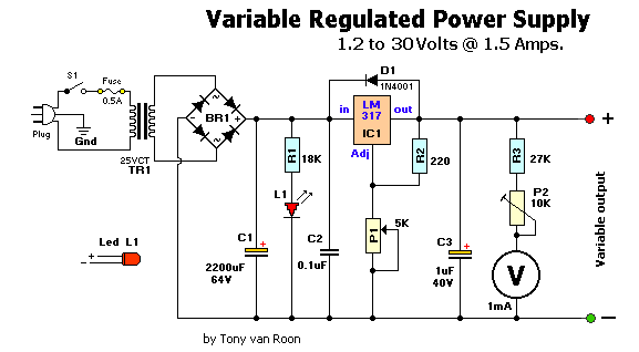
How to Build 1.2-30V/1.5A Variable Regulated Power supply, This is simple 1.2-30V/1.5A variable regulated power supply circuit diagram The 110V-AC coming from the powercord is fed to the transformer TR1 via the on-off switch and the 500mA fuse. The 30vac output (approximately) from the transformer is presented to the BR1, the bridge-rectifier, and here rectified from AC (Alternating Current) to DC (Direct Current). If you dont want to spend the money for a Bridge Rectifier, you can easily use four general purpose 1N4004 diodes. The pulsating DC output is filtered via the 2200µF capacitor (to make it more manageable for the regulator) and fed to IN-put of the adjustable LM317 regulator (IC1). The output of this regulator is your adjustable voltage of 1.2 to 30volts varied via the Adj pin and the 5K potmeter P1. The large value of C1 makes for a good, low ripple output voltage.

 1.2-30V/1.5A Variable Regulated Power supply Circuit Diagram

1.2-30V/1.5A Variable Regulated Power supply Circuit


Why exactly 1.2V and not 0-volt? Very basic, the job of the regulator is two-fold; first, it compares the output voltage to an internal reference and controls the output voltage so that it remains constant, and second, it provides a method for adjusting the output voltage to the level you want by using a potentriometer. Internally the regulator uses a zener diode to provide a fixed reference voltage of 1.2 volt across the external resistor R2. (This resistor is usually around 240 ohms, but 220 ohms will work fine without any problems). Because of this the voltage at the output can never decrease below 1.2 volts, but as the potentiometer (P1) increases in resistance the voltage accross it, due to current from the regulator plus current from R2, its voltage increases. This increases the output voltage.

D1 is a general purpose 1N4001 diode, used as a feedback blocker. It steers any current that might be coming from the device under power around the regulator to prevent the regulator from being damaged. Such reverse currents usually occur when devices are powered down.

The ON Led will be lit via the 18K resistor R1. The current through the led will be between 12 - 20mA @ 2V depending on the type and color Led you are using. C2 is a 0.1µF (100nF) decoupler capacitor to filter out the transient noise which can be induced into the supply by stray magnetic fields. Under normal conditions this capacitor is only required if the regulator is far away from the filter cap, but I added it anyway. C3 improves transient response. This means that while the regulator may perform perfectly at DC and at low frequencies, (regulating the voltage regardless of the load current), at higher frequencies it may be less effective. Adding this 1 µF capacitor should improve the response at those frequencies.

R3 and the trimmer pot (P2) alows you to zero your meter to a set voltage. The meter is a 30Volt type with an internal resistance of 85 ohms. I you have or obtained a meter with a different Ri (internal resistance) you will have to adjust R3 to keep the current of meter to 1mA. Just another note in regards this meter, use the reading as a guideline. The reading may or may not be off by about 0.75volts at full scale, meaning if your meter indicates 30 volts it may be in reality almost 31 volts or 29 volts. If you need a more precies voltage, then use your multimeter.


Construction:
Because of the few components you can use a small case but use whatever you have available. I used a power cord from a computer and cut the computer end off. All computer power cords are three-prong. The ground wire, which is connected to the middle pin of the power plug is connected to the chassis. The color of the ground-wire is either green or green/yellow. It is there for your protection if the 110vac accidentally comes in contact with the supply housing (case). BE CAREFUL always to disconnect the powerplug when you working inside the chassis. If you choose to use an in-line, or clip-type fuseholder be sure to isolate it with heat shrink or something to minimize accidental touching.

I use perf-board (or Vero board) as a circuit board. This stuff is widely available and comes relatively cheap. It is either made of some sort of fiber material or Phenolic or Bakelite pcb. They all work great. Some Phenolic boards come with copper tracks already on them which will make soldering the project together easier.

I mounted the LM317(T) regulator on a heatsink. If you use a metal/aluminum case you can mount it right to the metal case, insulated with the mica insulator and the nylon washer around the mounting screw. Note that the metal tab of the LM317 is connected internally to the Output pin. So it has to be insulated when mounting directly to the case. Use heat sink compound (comes in transparent or white color) on the metal tab and mica insulator to maximize proper heat transfer between LM317 and case/ or heatsink.

Drill the holes for the banana jacks, on/off switch, and LED and make the cut-out for the meter. It is best to mount everything in such a way that you are able to trouble-shoot your circuit board with ease if needed. One more note about the on-off switch S1, this switch has 110VAC power to it. After soldering, insulate the bare spots with a bit of silicon gel. Works great and prevents electrical shock through accidental touching.

If all is well, and you are finished assembling and soldering everything, check all connections. Check capacitors C1 & C3 for proper polarity (especially for C1, polarity reversal may cause explosion). Hookup a multimeter to the power supply output jacks. Set the meter for DC volts. Switch on S1 (led will light, no smoke or sparks?) and watch the meter movement. Adjust the potentiometer until it reads on your multimeter 15Volts. Adjust trimpot P2 until the meter also reads 15volts. When done, note any discrepancies between your multimeter and the power supply meter at full scale (max output). Maybe there is none, maybe there is a little, but you will be aware of it. Good luck and have fun building!


Parts List

BR1 = Bridge Rectifier, 100V - 3A       C1 = 2200 µF, 63V
IC1 = LM317, adjustable regulator       C2 = 0.1 µF
  V = Meter, 30V, Ri = 85 ohm           C3 = 1µF, 40V
TR1 = Transformer, 25V, 2A            Plug = 3-wire plug & cord
 R1 = 18K, 5%                           S1 = On-Off toggle switch
 R2 = 220 ohm, 5%                       D1 = 1N4001
 R3 = 27K, 5%                         Fuse = 110V, 500mA, slow-blow
 P1 = 5K, potentiometer               FuseHolder, wire, solder, case, knob for P1
 P2 = 10K, 10-turn trim-pot           Red & Black Banana Jacks

Notes:  
This is a simple, but low-ripple powersupply, and an excellent project if youre starting out in electronics. It will suit your needs for most of your bench testing and prototype applications. The output is adjustable from 1.2 volts to about 30 volts. Maximum current is about 1.5 amps which is also sufficient for most of your tinkering. It is relatively easy to build and can be pretty cheap if you have some or all the required parts. A printed circuit board is not included and Im not planning on adding one since the whole thing can easily be build on perferated or vero board. Or buy one of Radio Shack/Tandys experimentors boards (#276-150). Suit yourself. The meter and the transformer are the money suckers, but if you can scrounge them up from somewhere it will reduce the cost significantly. BR1 is a full-wave bridge rectifier. The two ~ denotes AC and are connected to the 25vac output coming from the transformer. IC1 is a 3-pin, TO-220 model. Be sure to put a cooling rib on IC1, at its max 1.5 A current it quickly becomes very hot..

All the parts can be obtained from your local Radio Shack or Tandy store. The physical size of the power supply case depends largely on the size of the meter & transformer. But almost anything will do. Go wild.


Sourced By  Tony  van roon
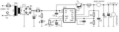
Simple 0 30 Volt Laboratory Power Supply

The linear power supply, shown in the schematic, provides 0-30 volts, at 1 amp, maximum, using a discrete transistor regulator with op-amp feedback to control the output voltage. The supply was constructed in 1975 and has a constant current mode that is used to recharge batteries. 

With reference to the schematic, lamp, LP2, is a power-on indicator. The other lamp (lower) lights when the unit reaches its preset current limit. R5, C2, and Q10 (TO-3 case) operate as a capacitor multiplier. The 36 volt zener across C2 limits the maximum supply voltage to the op-amps supply pins. D5, C4, C5, R15, and R16 provide a small amount of negative supply for the op-amps so that the op-amps can operate down to zero volts at the output pins (pins 6). 

A more modern design might eliminate these 4 components and use a CMOS rail-to-rail op-amp. Current limit is set by R3, D1, R4, R6, Q12, R10, and R13 providing a bias to U2 that partially turns off transistors Q9 and Q11 when the current limit is reached. R4 is a front panel potentiometer that sets the current limit, R22 is a front panel potentiometer that sets the output voltage (0-30 volts), and R11 is an internal trim-pot for calibration. The meter is a 1 milliamp meter with an internal resistance of 40 ohms. Switch S1 determines whether the meter reads 0-30 volts, or 0-1 amp. 

0-30 Volt Laboratory Power Supply Circuit diagram

 A more modern circuit might use a single IC regulator, such as the MC78XX, or MC79XX series, immediately after the half wave rectifier, to replace approximately 30 components, or at least a high precision zener diode to replace D10 as the voltage reference. The LM4040 is one such voltage reference and has excellent stability over temperature. IC regulators such as the MC78XX series may eventually become obsolete as newer IC regulators are designed, however, discrete transistors, op-amps, and zeners are more generic, have a longer production lifespan, and allow the designer to demonstrate that he understands the principles of linear regulated power supply operation.Link