Thursday, November 20, 2014

65W Power Amplifier Circuits with HEXFET

65W65W Power Amplifier Circuits with HEXFET

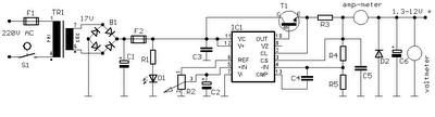
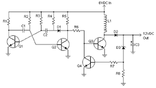
A average ability amplifier that is characterized by a lot of acceptable complete quality, but accompanying is actual simple in the construction. Him uses, abundant time in my alive loudspeakers. In his achievement date abide the actual acceptable FET transistors, technology HEXFET, transistor which are controlled by voltage and no by accepted as the classically bipolar transistors. The ambit has balanced designing, absolute appropriately the harmonic baloney problem.

All the transistors that are acclimated in the ambit are simple and they abide in big clearings in the market. The pairs of cogwheel amplifiers Q1-2 and Q3-4 should be akin amid them and abreast the one in the other. Appropriately you can buy abundant transistors of types BC550C and BC560C, and with a multimeter you bout amid them creating pairs with aforementioned characteristics, ensuring appropriately compatible behavior in the temperature changes etc. Networks RC from the R7/C3 and R12/C4 abatement the bandwidth of cogwheel amplifiers and ability amplifier in the 6.5MHZ. Resistors R8-9-10-11 action as bounded acknowledgment in the cogwheel amplifiers convalescent the linearity. The cogwheel amplifiers are supplied with connected accepted from him accepted sources Q5 and Q6. The bent of accepted sources becomes from the aggregate of diodes LED D1, D2 and R20.

This becomes because the aggregate transistor/LED ensures big thermic stability, for this acumen should they are in actual abreast ambit [1]. With the TR1 trimmer we adapt the bent accepted of achievement ability stage. For this acumen Q8 should acquisition itself on the heatsink so that it ensures thermic adherence in the bias, so that it does not change with the temperature changes. The resistors R32-33 appearance a bounded acknowledgment bronchus in the achievement stage, because this functions as voltage amplifier.

With the TR1, R3-4, C14 we adapt the amplifier achievement DC account voltage, abreast in the zero. The transistors Q8-10-11-12-13, [Fig.1] should are placed on heatsink, abacus amid the transistors and the heatsink of acceptable affection leaves mica and ointment. Inductor L1 is constituted by 6 coils of cloistral cupreous wire of bore 1.5mm, with centralized inductor bore of 16mm

1 3V DC to 12 2V DC Regulator Power Supply

Power supply circuit to generate output below were variations between 1.3V DC to 12.2V DC with 1A current.
In addition, the power supply circuit is also equipped with over-current protection or shield against belebih flow. Power supply circuit is very simple, but the quality is quite good, made her basiskan regulator IC LM723 is a pretty legendary.


1.3V


Description:

R2 to set the output voltage. The maximum current is determined by R3, over-current protection circuit inside the LM723 to detect the voltage on R3, if it reaches 0.65 V, the voltage output will be off her. So the current through R3 can not exceed 0.65 / R3 although output short-circuit in his.

C3 and C4 are ceramic capacitors, as much as possible directly soldered to the PCB, this is because the LM723 is prone to oscillation that is not cool.

LM723 works with 9.5V input voltage to 40 V DC and the LM723 can generate its own current of 150mA when the output voltage is not more than 6-7V under input voltage.


Specifications:

Output (value estimated):

Vmin = (R4 + R5) / (R5 * 1.3)
Vmax = (7.15 / R5) * (R4 + R5)
Imax = 0.65/R3
Max. Power on R3: 0.42/R3


Min. DC Input Voltage (pin 12 to pin 7): Vmax + 5

Component List:

B1 40V/2.5A
C1 2200uF (3300uF even better)
C2 4.7uF
C3 100nF
C4 1NF
C5 330nF
C6 100uF
Green LED D1
D2 1N4003
F1 0.2A F
F2 2A M
IC1 LM723 (in a DIL14 plastic package)
R1 1k
R2 Pot. 5k
R3 0.56R/2W
R4 3.3k
R5 4.7k
S1 250V/1A
T1 2N3055 on a heatsink 5K / W
TR1 220V/17V/1.5

SMS Remote controller circuit

SMS Remote controller is a device used to control a device remotely using SMS through GSM mobile phones. Process control equipment with a series of AVR ATTiny To SMS Remote Controller can be used to control life and death of these equipment will provide information on the status of replies to our phone in return successful command execution. 
Equipment can be controlled by a series of AVR ATTiny To SMS Remote Controller include lights, water pumps, garage doors, gates and much more. AVR series ATTiny To SMS Remote controller uses the module-47 Sony ericson GM as recipient and sender of the SMS module. Then to the SMS data processor on a series of AVR ATTiny To SMS Remote controller is using AVR microcontroller ATTiny 2313.


Series AVR ATTiny To SMS Remote Controller

SMS Remote controller circuit Click to view larger. 

AVR circuit this part ATTiny To SMS Remote Controller
AVR series ATTiny To SMS Remote controller uses the AVR attiny2313 with 4MHz clock frequency, GSM Module GM trnceiver 47 Sony ericson, SIM Card, 4 relays and an IC regulator. ATTiny AVR microcontroller 2313 can work well on the voltage 2.7 VDC - 5.5 VDC for working with the frequency at 10MHz bahwah. 

The set of AVR ATTiny In SMS Remote Controller To make use of this power supply from the batteries 3.3 VDC. Connection using a SIM Card SIM Card Holder which is connected to the module GM-47, AVR series ATTiny To SMS Remote Controller works with communication between AVR ATTiny and GM-47 module at 9600bps. In a series of AVR ATTiny To SMS Remote controller is equipped with LED D6 as an indicator of the data interconnect GM-47 module with cellular operators where this LED will light continuously when not apat network and will be lit by flashes when a signal from the operator.

Specifications AVR series ATTiny To SMS Remote Controller
  • 4 Relay for ON / OFF electronic devices
  • 8 input lines for reading in a normal switching
  • LED indicators signal operator
  • SMS command with password, so only the owner can operate

Guitar Amplifier Circuit Diagram 100W

GuitarGuitar Amplifier Circuit Diagram 100W

The ability amp lath has remained banausic back it was aboriginal appear in 2002. It absolutely isn’t broken, so there’s no acumen to fix it. The photo beneath shows a absolutely accumulated lath (available as apparent as M27). Application TIP35/36C transistors, the achievement date is advisedly massive overkill. This ensures believability beneath the best backbreaking date conditions. No amplifier can be fabricated allowed from everything, but this does appear close.

The ability amp (like the antecedent version) is about based on the 60 Watt amp ahead appear (Project 03), but it has added accretion to bout the preamp. Other modifications accommodate the abbreviate ambit aegis – the two little groups of apparatus abutting to the bent diodes (D2 and D3). This new adaptation is not massively altered from the original, but has adjustable bias, and is advised to accommodate a “constant current” (i.e. aerial impedance) achievement to the speakers – this is accomplished application R23 and R26. Note that with this arrangement, the accretion will change depending on the amount impedance, with lower impedances giving lower ability amp gain. This is not a problem, so may cautiously be ignored.

Should the achievement be shorted, the connected accepted achievement appropriate will accommodate an antecedent akin of protection, but is not absolutely foolproof. The abbreviate ambit aegis will absolute the achievement accepted to a almost safe level, but a abiding abbreviate will account the achievement transistors to abort if the amp is apprenticed hard. The aegis is advised not to accomplish beneath accustomed conditions, but will absolute the aiguille achievement accepted to about 8.5 Amps. Beneath these conditions, the centralized fuses (or the achievement transistors) will apparently draft if the abbreviate is not detected in time.

Wednesday, November 19, 2014

Broken Charger Detector

With this circuit we can detect when charger wire was broken. This detector will work when the charger wire damage the detector will sounds an alarm warning. So we can know the charger wire is broken.


As long as there is a little current flows from the charger to battery the diodes D1 and D2 will conduct.This forward voltage drop of 1.4 V across the diodes make the Q2 ON.So the transistor Q1 will be OFF.When there is no at all any current flowing (when the wire is broken or there is a loose contact) there will not be any drop across D1&D2 and so Q2 will be OFF.This makes the Q1 ON,the buzzer beeps and the LED glows.

Voltmeter and ampere meter using PIC

volt meter and ampere meter with PIC can be used to measure voltage and current simultaneously. The series of volt meter and ampere meter with PIC uses a PIC16F876A as a data processor voltage and current are measured. This circuit uses the LCD 16 × 2, which is used to display data voltage and current measurements. In the article volt meter and ampere meter with PIC are discussed only limited to hardware only. For more details can be seen from the image volt meter and ampere meter with PIC .
 
 
In the circuit volt meter and ampere meter with PIC above used 3 pieces of buttons for setting Calibration measurement data. The circuit is basically working with the source voltage 5VDC. 

Turbo Bass Circuit

Turbo
Turbo Bass Circuit

PWM DC Motor Driver

As the title "PWM DC Motor Driver with Forward / Reverse and Breaking" this series is a PWM DC motor controller that can control DC motors with clockwise rotation and counter-clockwise and is equipped with a braking system. In a series DC motor control PWM DC Motor Driver with Forward / Reverse and Breaking use this system for SASL PWM DC motor rotation speed. Power driver in a series DC motor PWM DC Motor Driver with Forward / Reverse and Breaking uses mosfet IRF150. Then, to control the direction of rotation of DC motor in the circuit of PWM DC Motor Driver with Forward / Reverse and Breaking uses relays. Then the braking system on a series of PWM DC Motor Driver with Forward / Reverse and Breaking is done by a resistor that is connected to the motor using relays.

Fig circuit PWM DC Motor Driver with Forward / Reverse and Breaking


See image details a series of PWM DC Motor Driver with Forward / Reverse and Breaking above. DC motor speed is set to pulse through the input PWM PWM, Power driver uses and the protection mosfet IRF150 with D7 as dumping. Then to start and stop is controlled via the logic input lines provided on the start / stop circuit PWM DC Motor Driver. Line inputs are used to set the reverse direction of rotation of DC motor that is with merberikan logic 1 / 0 on the path. R19 in the circuit of PWM DC Motor Driver serves as an expense to do the braking circle DC motor.

Light Switch for Lamps Controller

Light switch series with photo transistor above can be used to control garden lights, street lights, or night lamps automatic. Light switches can be made from several kinds of light sensors. The circuit of light switches are made using a photo transistor light sensors. The series of light switches or light control switch is very simple, because it is made with 1 piece of transistors, 1 piece of photo transistor, 1 relay, 1 variable resistors and diodes.
The series of light switches can work on the voltage 6-12 VDC or DC voltage that judgments in accordance with the relay is used. To set the sensitivity of the exposure is set by VR1.  Light switch series with photo transistors can be used to control some lights in parallel with the power depends on the ability of the relay is used.

Circuit of  Light switch


Tuesday, November 18, 2014

Guitar Control Circuit Diagram

GuitarGuitar Control Circuit Diagram

Device purpose:

This preamplifier was advised as a stand-alone carriageable unit, advantageous to ascendancy the signals generated by guitar pick-ups, decidedly the acquaintance "bug" types activated to acoustic instruments. Obviously it can be acclimated with any blazon of apparatus and pick-up.

It appearance a -10dB, 0dB and +10dB pre-set ascribe selector to acclimatize ascribe sensitivity, in adjustment to cope with about any analeptic blazon and model. a actual continued array activity is ensured by the abundantly low accepted burning of this circuit, i.e. beneath than 800µA.

Circuit operation:

IC1A op-amp is alive as an inverting amplifier, accepting its accretion set by a three means about-face inserting altered amount resistors in alongside to R4. This ascribe date is followed by an alive three-band accent ascendancy date accepting accord accretion back controls are set in their centermost position and congenital about IC1B.

IR Infra Red Sensor with 7 Segment Display

Infrared light has a difference with ordinary light in general. We can see clearly when a light or light on an object.
As with the infrared light we can not see the manifestation of these rays. Frankly I can not answer when asked why the infrared rays are not visible in the eyes of us. So at night do not hope you can make light by using infrared light. One thing that is often heard from many people that infrared light can utilized for the functions of a camera that can see in dark conditions is often called an infrared camera.

Actually I have explained the working principles of electronic circuit section in this blog is about the basic working principle of a series of infrared sensors are simple. To design this sensor circuit you should not find trouble if you ever make another series of sensors. Its just that the sensor circuit consists of the transmitter and receiver, to learn the basic principles of this series of infrared you can see in the Basic Principles Series Infrared Transmitter and Receiver. In the circuit this time I try to utilize the output of this sensor circuit as a trigger circuit counter or counters.
IR

Picture series of infrared sensors | infrared sensor circuit scheme


Component List:

1. Resistors: R1 (33K), R2 (1K), VR1 (Potensio 100K)
2. Capacitors: C1 (100nF)
3. Transistors: Q2 (BC547 should)
4. Photo transistor: Q1
5. IC: 40 106 (Schimitt trigger), 4026 (Decade counter)
6. 7-Segment

WORKING PRINCIPLE:

In the transmitter circuit arrangement so that our task is only an infrared LED lights up and no shortage or excess of power, therefore, use 680 ohm resistors. On The set of photo transistor receiver serves as a useful tool sensor sensed a change in the intensity of infrared light. When infrared light is not on the photo transistor, the photo transistor is like a switch is open so that the transistor is in cutoff position (open). Because the collector and emitter open it in accordance with the laws of the voltage divider, the collector emitter voltage equal to supply voltage (logic high). The output of these collectors would make a series of counter counting irregularly if we did not dampen the bounce output to the input couinter. To reduce the bounce and clarify the logic signal to be our input to counter circuit, we use Schmitt trigger ignition. Schmitt trigger ignition is very useful for those of you who relate to digital circuits, eg, using the damping bounce of mechanical switches on the input digital circuit.

The series of counters that I use here is to use IC 4026 (Decade Counter), one of the family ic CMOS. IC counter counts up if this will get the clock input changes from logic low to high. This IC can directly connect it to the seven segment because the output is designed for seven segment mmang. So you do not need to use as a modifier decoder IC binary value into a score of 7-segment.
To menmgatur you can rotate the sensor sensitivity potensio VR1 at a critical point, or if necessary you can replace R2 with a more appropriate value.

6 to 12 Volt Converter

Below its a converter circuit voltage from 6 Volt to 12 Volt DC.

6
6 Volt to 12 Volt DC

Part List :
R1, R4 2 .2K 1/4W Resistor
R2, R3 4.7K 1/4W Resistor
R5 1K 1/4W Resistor
R6 1.5K 1/4W Resistor
R7 33K 1/4W Resistor
R8 10K 1/4W Resistor
C1,C2 0.1uF Ceramic Disc Capacitor
C3 470uF 25V Electrolytic Capcitor
D1 1N914 Diode
D2 1N4004 Diode
D3 12V 400mW Zener Diode
Q1, Q2, Q4 BC547 NPN Transistor
Q3 BD679 NPN Transistor
L1 See Notes
Notes
1. L1 is a custom inductor wound with about 80 turns of 0.5mm magnet wire around a toroidal core with a 40mm outside diameter.

2. Different values of D3 can be used to get different output voltages from about 0.6V to around 30V. Note that at higher voltages the circuit might not perform as well and may not produce as much current. You may also need to use a larger C3 for higher voltages and/or higher currents.

3. You can use a larger value for C3 to provide better filtering.

4. The circuit will require about 2A from the 6V supply to provide the full 800mA at 12V.

Phone Busy Indicator Diagram

PhonePhone Busy Indicator Diagram

Have you anytime been application the modem or fax and addition abroad picks up the phone, breaking the connection? Well, this simple ambit should put an end to that. It signals that the buzz is in use by lighting a red LED. When the buzz is not in use, a blooming LED is lit. It needs no alien ability and can be affiliated anywhere on the buzz line, alike army central the phone.
Notes

1. This is a very simple circuit and is easily made on a perf board and mounted inside the phone.

2. LED1 and LED2 flash on and off while the phone is ringing.

3. Do not worry about mixing up the Tip and Ring connections.

4. The ring voltage on a phone line is anywhere from 90 to 130 volts. Make sure no one calls while you are making the line connections or youll know it. :-)

5. In some countries or states you will have to ask the phone company before you connect this to the line. It might even require an inspection.

6. If the circuit causes distortion on the phone line, connect a 680 ohm resistor in between one of the incoming line wires and the bridge rectifier.

Phone Busy Indicator Diagram Part List

R1 1 3.3K 1/4 W Resistor
R2 1 33K 1/4 W Resistor
R3 1 56K 1/4 W Resistor
R4 1 22K 1/4 W Resistor
R5 1 4.7K 1/4 W Resistor
Q1, Q2 2 2N3392 NPN Transistor
BR1 1 1.5 Amp 250 PIV Bridge Rectifier
LED1 1 Red LED
LED2 1 Green LED
MISC 1 Wire, Case, Phone Cord

Magnetic Detector

Magnetic switch is a circuit which can respond to magnetic fields that were around the sensor. The series of magnetic switches uses sensors in the form of limit switches that provide an additional metal plate that can respond to a magnet. Magnetic switch circuit is made with an NE555 monostable multivibrator and a flip-flop togle from IC CD4013. The series of magnetic switches uses 12VDC supply voltage and the magnetic circuit is mounted indicator switch which serves to give a signal when the sensors respond to magnetic fields using the LED D1.


Click Image for full image

If the limit switches (sensors), active (connected) then it will get multivibrator NE555 triger signal and provides output pulses to be used to provide input signals to the flip-flop togle Relay K1 and active. Then when the sensors (limit switches respond to the magnetic field again, the multivibrator will give togle pulse as input to the flip-flop relay K1 and non-active.

Monday, November 17, 2014

Loudspeaker Driver Circuit

The series of loudspeaker drivers are electronic circuits that function to bridge between high-output circuit with a loudspeaker berimpedasi berimpedansi low. 


Loudspeaker

Why this driver is needed so that the output voltage to be inserted into the loudspeaker is not impaired. Declining value of this voltage is very possible given the lack of rules regarding the distribution of voltage and resistance instead of parallel. Where every prisoner that is placed parallel with other prisoners or the inmates totally substitute for detainee custody is smaller than with individual prisoners themselves. For example, 10 ohm resistance 10 ohms paralleled with the prisoners would get custody instead of 5 ohms. Resistivity 10 ohm to 100,000 ohm paralleled the total resistance is 9.9990 ohms. So it can be concluded that the total voltage will always be smaller than the origin of each detainee. Then, with a decrease in resistance (only using a combination of resistors) or the impedance of the output terminals before, then in accordance with the laws of the voltage divider in series can be ascertained that the prisoners connect in series with output terminal will have a larger part of the voltage and output terminal itself will decline voltage.

The working principle speaker driver circuit is actually very simple and easy to understand. Where the input signal is only used as a trigger to move the second driver transistor to the rhythm of the input signal. While the current that would flow to the loudspeaker most of the power supply driver circuit. You could say similar to the use of transistors as switches. Therefore, in this speaker series driver not found a combination of resistors for reinforcement. So if we look at the picture above, so most of the current flowing in the loudspeaker load is derived from the 9 volt supply voltage, instead of the input ac signal, so that the input signal will not be burdened.

System circuit not Minimum Evaluation Board AT89C2051 and AT89C4051

Maybe we are more familiar with the term Minimum System AT89C2051 circuit, but this time I present a circuit which is not only a series of Minimum System AT89C2051 but more than that.
System

The circuit is more deserves to be called Evaluation Board AT89C2051 and AT89C4051. Some of the advantages of circuit Minimum System AT89C2051 / AT89C2051 and AT89C4051 Evaluation Board which I was present this time, hardware-hardware support below:


RS-232 interface, DB-9
Header for LCD display
I2C, PCF8574 I / O extender
AT24C04, I2C EEPROM

MP3 Car Amplifier Schematic Circuits 150W

MP3MP3 Car Amplifier Schematic Circuits 150W

These accessories are low cost, aerial speed, bifold JFET ascribe operational amplifiers with an internally akin ascribe account voltage (BI-FET II technology). They crave low accumulation accepted yet advance a ample accretion bandage amplitude artefact and fast bulk rate. In addition, able-bodied akin aerial voltage JFET ascribe accessories accommodate actual low ascribe bent and account currents. The LF353 is pin accordant with the accepted LM1558 acceptance designers to anon advancement e the all-embracing achievement of absolute LM1558 and LM358 designs. These amplifiers may be acclimated in applications such as aerial acceleration integrators, fast D/A converters, sample and authority circuits and abounding added circuits acute low ascribe account voltage, low ascribe bent current, aerial ascribe impedance, aerial bulk amount and advanced bandwidth. The accessories additionally display low babble and account voltage drift. (National Semiconductor

Internally trimmed offset voltage: 10 mV
Low input bias current: 50pA
Low input noise voltage: 25 nV
Low input noise current: 0.01 pA
Wide gain bandwidth: 4 MHz
High slew rate: 13 V/us
Low supply current: 3.6 m
High input impedance: 1012.
Low total harmonic distortion : <>

IC LM2917 Frequency to Voltage Converter

IC LM2917 IC chip is designed specifically as a Frequency to Voltage Converter or Frequency to Voltage converter. In its use to applications Frequency to Voltage Converter IC LM2917 requires few external components. There are several examples of applications of Frequency to Voltage Converter IC LM2917 datasheet that is included in the LM2917 IC. In this article series Frequency to Voltage Converter IC also taken from the LM2917 datasheet. The advantages of single chip LM2917 Frequency to Voltage Converter is able to provide instantaneous volt output o at time of frequency change 0 Hz. Very easy to apply in measuring the output frequency with the formulation of single-chip Frequency to Voltage Converter VOUT = FIN x VCC x R1 x C1. Then the single-chip LM2917 Frequency to Voltage Converter This configuration requires only the RC only in frequency doubling. And has an internal zener regulator to aimlessly accuracy and stability in frequency-to-voltage conversion process.

Application circuit Figure IC LM2917 as Frequency to Voltage Converter

IC


Feature-owned single-chip LM2917 Frequency to Voltage Converter
Reference to ground directly with variable reluctance
Op Amp / Comparator with transistor output
50 mA maximum output currents for application directly to the load
Frequency doubling for low ripel
Buid in zener
Linear output ± 0.3%
Application single chip LM2917 Frequency to Voltage Converter
Frequency to Voltage Converter
Rotation speed sensor applications
Speedometer
Tachometer
Cruise Control
Cluth Control
And other applications associated with the measurement of rotation speed or frequency measurements.

Condenser Pre Amplifier LM 1458

This is a simple preamplifier circuit for electret condenser microphone.
using a LM1458 dual op amp IC. The circuit takes the audio signal rom the condenser microphone and amplifier it, so you can use the microphone as the input to some device which wouldn’t normally accept microphone level signals .

Condenser


Schematic Circuit of Microphone Electret

Condenser Pre Amplifier


The circuit requires a 6-9 volt supply. Output of the microphone amplifier can be made variable by connecting a 10kΩ potentiometer . Circuit’s gain can be increased by men perbesar the value of 47K, depending on the input sensitivity of the main amplifier system. The microphone should be housed in a small round enclosure.
List componet of condenser pre-amp mic circuit

Q1,Q2    : LM1458 Op-Amp
R1,R2,R3 : 4.7k ohm resistor
R4, R5   : 10k ohm resistor
R6,R7    : 47k ohm resistor
C1,      : 0.22uF ceramic capacitor
C2       : 1uF ceramic capacitor

Absolute maximum ratings of LM 1458 IC

Supply Voltage               :  ±18V
Power Dissipation            : 400 mW
Differential Input Voltage   : ±30V
Input Voltage                : ±15V
Output Short-Circuit Duration: Continuous
Operating Temperature Range  : 0°C to +70°C
Storage Temperature Range    : −65°C to +150°C
Lead Temperature             :(Soldering, 10 sec.) 260°C

Sunday, November 16, 2014

Power supply using tube Z2C

Power supply using tube Z2C are designed specifically to provide power supply voltage to the EL-34 tube amplifier push-pull in the previous article. Power supply with Z2C tube to tube power amplifier is made with a tube rectifier Z2C.
Just as the power supply for power amplifier tubes previously, the power supply is also using a filter with 3 levels of electrolytic capacitors. The circuit power supply with tube rectifier can deliver Z2C +210 VDC output voltage.
Power
Z2C on the rectifier tube in power supply with tube above requires a supply voltage for the filaments taken from the other side of the transformer secondary. Z2C tube power supply with a power supply that is used as a substitute DAPT power supply for power amplifier tubes with a diode

Saturday, November 15, 2014

LOGIC GATES

Logic gates are the devices used as basic building blocks of all the digital circuits. The basic logic gates are NOT, AND and OR along with NOR, NAND, EX-OR etc. We have to use different laws, rules and theorems to analyze the digital circuits. By connecting the gates mentioned earlier, in different ways, we can build circuits that can perform arithmetic and other functions associated with human brain. Because they simulate mental processes, gates are often called as logic circuits.

A logic Gate is an electronic circuit having one or more than one inputs and only one output. The relationship between the input and the output is based on a "certain logic". Based on this logic gates are named as NOT gate, AND gate, OR, NAND, NOR etc.

CLASSIFICATION OF LOGIC GATES:

LOGIC GATES
Basic Gates
Universal Gates
Derived Gates
  •       NOT Gate
  •       AND Gate
  •       OR Gate
  •       NAND Gate
  •       NOR Gate
  •       EX-OR Gate
  •       EX-NOR Gate


NOT GATE | INVERTER

The NOT gate or Inverter is a logic gate having one input (A) and one output (Y). It is called "Inverter" because its output is the inverted version or "complement of its input. This is shown in the truth table of NOT gate.

Truth Table
Input A
Output Y
0
1
1
0


Symbol
Equivalent Circuit


A is input while Y is the output.
The bubble (o) in the symbol of a NOT gate indicates inversion. The operation of a NOT gate for various input combinations is as shown in above figure.


AND GATE

AND is one of the logic operators. It performs the logical multiplication on its inputs. The output is high (Y=1) if and only if all the inputs to the gate are high (1). The output is low (0), if atleast one of the inputs is low (0). AND gate can have two or more inputs and only one output.

Symbol
Logical Symbol


Truth Table
Inputs
Outputs
A
B
Y
0
0
0
0
1
0
1
0
0
1
1
1


Boolean Expression
The expression relating the inputs and output of a gate is called as the Boolean expression. The Boolean expression. The Boolean expression for an AND gate is;
Y = A.B
where the "dot" between A and B represents multiplication.
By substituting different values of A and B into the Boolean expression we can get the corresponding state of output. This is how we can verify the truth table of the gate.


OR GATE

An OR gate performs the logical addition on its inputs therefore its output will be high (1) if any one or both the inputs are high (1). Its output will be low (0) if and only if both the inputs are simultaneously low (0).

Logic Symbol
Logical Symbol


Truth Table
Inputs
Outputs
A
B
Y
0
0
0
0
1
1
1
0
1
1
1
1
Boolean Expression
The Boolean expression for a two input OR gate is;
Y = A + B
By substituting different values of A and B into this expression we can get the corresponding output. This is how we can verify the truth table of a gate.

Friday, November 14, 2014

STABILIZED POWER SUPPLY 3 30 V 2 5 A

This is a versatile power supply that will solve most of the supply problems arising in the everyday work of any electronics workshop. It covers a wide range of voltages being continuously variable from 30 V down to 3 V. The output current is 2.5 A maximum, more than enough for most applications. The circuit is completely stabilised even at the extremes of its output range and is fully protected against short-circuits and overloading.

Circuit Diagram


Working

The power supply is using a well known and quite popular VOLTAGE STABILIZER IC the LM 723. The IC can be adjusted for output voltages that vary continuously between 2 and 37 VDC and has a current rating of 150 mA which is of course too low for any serious use. In order to increase the current handling capacity of the circuit the output of the IC is used to drive a darlington pair formed by two power transistors the BD 135 and the 2N 3055. The use of the transistors to increase the maximum current output limits the range of output voltages somewhat and this is why the circuit has been designed to operate from 3 to 30 VDC. The resistor R5 that you see connected in series with the output of the supply is used for the protection of the circuit from overloading. If an excessively large current flows through R5, the voltage across it increases and any voltage greater than 0.3 V across it has as a result to cut the supply off, thus effectively protecting it from overloads. This protection feature is built in the LM 723 and the voltage drop across R5 is sensed by the IC itself between pins 2 and 3. At the same time the IC is continuously comparing the output voltage to its internal reference and if the difference exceeds the designer’s standards it corrects it automatically. This ensures great stability under different loads. The potentiometer P1 is used to adjust the out put voltage at the desired level. If the full range from 3 to 30 V is desired then you should use a mains transformer with a secondary winding having a rating of at least 24 V/3 A. If the maxi mum voltage output is not desired you can of course use a transformer with a lower secondary voltage output. (However, once rectified the voltage across the capacitor C2 should exceed by 4-5 volts the maximum output expected from the circuit.

Parts List

Resistors
R1 = 560R 1/4W
R2 = 1,2 K 1/4W
R3 = 3,9 K 1/4W
R4 = 15K 1/4W
R5 = 0,15R 5W 

Capacitors
C1 = 100nF
C2 = 2200uF 35-40V
C3 = 100 pF
C4 = 100uF/ 35V

Miscellaneous
D = B40 C3300/2200, 3A Rectifier Bridge
P1 = 10K Potentiometer
TR1 = BD 135
TR2 = 2N3055
IC = LM723

BD 135


2N3055


LM723

DC MOTOR REVERSING CIRCUIT

When the forward button is pressed and released the motor will run continuously in one direction. The reverse button will cause the motor to run continuously in the opposite direction. The motor cannot be switched from forward to reverse unless the stop switch is pressed first and vice versa. Putting a motor straight into reverse would be quite dangerous, because when running a motor develops a back emf voltage which would add to current flow in the opposite direction and probably cause arcing of the relay contacts.

Circuit Diagram


Note

At first glance this may look over-complicated, but this is simply because three non-latching push button switches are used. When the forward button is pressed and released the motor will run continuously in one direction. The Stop button must be used before pressing the reverse button. The reverse button will cause the motor to run continuously in the opposite direction, or until the stop button is used. Putting a motor straight into reverse would be quite dangerous, because when running a motor develops a back emf voltage which would add to current flow in the opposite direction and probably cause arcing of the relay contacts. This circuit has a built-in safeguard against that condition. 

Circuit Operation 

Assume that the motor is not running and that all relays are unenergized. When the forward button is pressed, a positive battery is applied via the NC contacts of B1 to the coil of relay RA/2. This will operate as the return path is via the NC contacts of D1. Relay RA/2 will operate. Contacts A1 maintain power to the relay even though the forward button is released.
Contacts A2 apply power to the motor which will now run continuously in one direction. If now the reverse button is pressed, nothing happens because the positive supply for the switch is fed via the NC contact A1, which is now open because Relay RA/2 is energized. To Stop the motor the Stop switch is pressed, Relay D operates and its contact D1 breaks the power to relays A and B, (only Relay A is operated at the moment). If the reverse switch is now pressed and released. Relay B operates via NC contact A1 and NC contact D1. Contact B1 closes and maintains power so that the relay is now latched, even when the reverse switch is opened. Relay RC/2 will also be energized and latched. Contact B2 applies power to the motor but as contacts C1 and C2 have changed position, the motor will now run continuously in the opposite direction. Pressing the forward button has no effect as power to this switch is broken via the now open NC contact B1. If the stop button is now pressed. Relay D energizes, its contact D1 breaks power to relay B, which in turn breaks power to relay C via the NO contact of B1 and of course the motor will stop. All very easy. The capacitor across relay D is there to make sure that relay D will operate at least longer than the time relays A,B and C take to release.

Correction to Diagram

In the original circuit when the Stop switch was pressed, relay RA remains energized, its holding current path is through relay coils RB and RC. To fix this relay D has two contacts, D2 now breaks power to the relay coil.

Thursday, November 13, 2014

The programming of Propeller IC

Parallax, well known for its successful Basic Stamp IC, has recently introduced the Propeller: a new microcontroller with a certain difference. It packs no less than eight 32-bit processors (referred to as COGs in Propeller jargon) into a single package with only 40 pins. That design takes genuine simultaneous multiprocessing possible, and the sophisticated internal structure of the device makes it relatively easy to implement video and signal-processing applications. The Propeller can be programmed in assembly language or the high-level Spin language. The processor and the programming tools were developed entirely in-house by Parallax, with the hardware being designed from scratch starting at the transistor level. 
Programming The Propeller IC Circuit Diagram

The basic idea behind that was to avoid becoming involved in all sorts of patent disputes with other manufacturers. The result is astounding, and for software developers it certainly requires a change in mental gears. As is customary with modern microprocessors, the Propeller has a simple serial programming interface. The developer’s toolkit from Parallax has a modern USB port for that purpose, but a reasonably simple alternative (illustrated here) is also possible for anyone who prefers to work with the familiar RS232 port. Don’t forget that the Propeller works with a 3.3-V supply voltage.
Author: unknown - Copyright: Elektor Electronics

555 timer bassed Metal detector circuit with explanation

A very simple metal detector electronic project can be designed using a simple 555 timer integrated circuit . As you can see in the schematic circuit , this electronic project requires few external electronic parts .

This circuit detects metal and also magnets. When a magnet is brought close to the 10mH choke, the output frequency changes.
This metal detector project can be powered from a power supply that can provide an output DC voltage between 6 an 12 volt .
If a metal is closer to the L1 coil , will produce a change of output oscillation frequency, that will generate a sound in the 8 ohms speaker .

Metal

readmore: electroniq.net/other-projects/detectors/metal-detector-using-555-timer-circuit.html

Ceiling fan wiring diagram with capacitor connection

Simple Wiring diagram of ceiling fan


ceiling
Fig-1:  Ceiling fan wiring diagram

This is a simple illustrated circuit diagram of ceiling fan. To be noted that the wiring diagram is for AC 220V single phase line with single phase ceiling fan motor. Here a simple SPST switch is used to supply power or not to the fan motor and a Regulator is used to controlling the fan speed. Though it is very simple, but one thing to be noted that Switch and Regulator should be connected with the phase line of main power, not neutral.

You may like to see ceiling fan regulator circuit to controlling fan speed

Capacitor connection diagram of ceiling fan

Ceiling fan has a “capacitor start motor” in its inside. AC single phase capacitor start motor has two winding; one is starting winding and another is running winding.

ceiling
Fig-2:  Ceiling fan capacitor connection diagram

As it is a capacitor start-capacitor run type motor; there a capacitor is used in series with Starting Winding, It defines the direction of rotation. It is an electrolytic capacitor.

Sometimes you may have faced this type of question...

  1. Why ceiling fan rotating in reverse?
  2. What makes a ceiling fan run backwards?
Two of this question sounds the same; the answer of the both question is “If capacitor is connected with running winding/main coil instead of starting winding/auxiliary coil then the direction of rotation will changed. That’s mean if you want to change the direction of rotation of the fan, just connect the capacitor with other winding.

Lamp Flasher Portable circuit

 lamp flasher portable circuit
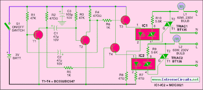
Here is a portable, high-power incandescent electric lamp flasher. It is basically a dual flasher (alternating blinker) that can handle two separate 230V AC loads (bulbs L1 and L2). The circuit is fully transistorised and battery-powered. The free-running oscillator circuit is realised using two low-power, low-noise transistors T1 and T2. One of the two transistors is always conducting, while the other is blocking.

Due to regular charging and discharging of capacitors C1 and C2, the two transistors alternate between conduction and non-conduction states. The collector of transistor T1 is connected to the base of driver transistor T4 through current-limiting resistor R5. Similarly, the collector of transistor T2 is connected to the base of driver transistor T3 through limiting resistor R6. These transistors are used to trigger Triac1 and Triac2 (each BT136) through optotriacs IC1 and IC2, respectively, and switch on the power supply to external loads L1 and L2.
IC1 and IC2 operate alternatively at a low frequency determined by the values of capacitors C1 and C2. The oscillator circuit built around transistors T1 and T2 generates low frequencies. When transistor T3 conducts, IC1 is enabled to ire Triac1 and bulb L1 glows. Similarly, when transistor T4 conducts, IC2 is enabled to ire Triac2 and bulb L2 glows. Connect the power supply line (L) of mains to bulbs L1 and L2, and neutral (N) to T1 terminals of Triac1 and Triac2.


You can also connect neutral (N) line of the external 230V mains supply to both loads (bulbs L1 and L2) as a common line and then route supply line (L) to respective loads (bulbs L1 and L2). The circuit works off only 3 volts. Since current consumption is fairly low, two AA-type cells are suficient to power the circuit. Assemble the circuit on a general-purpose PCB and enclose in a suitable plastic cabinet with integrated AA-size pen-light cell holder. Drill holes for mounting the ‘on’/‘off’ switch and power switching terminals. Also connect two bulb holders for bulbs L1 and L2.

Clap Switch Circuit Project

This is a simple electronics circuit of clap switch project. If you are a beginner electronics learner, and love to get new project experiment then this is a great circuit for you.  This circuit can on/off a 220V electronic device like fan, lamp by the sound of clap.

Circuit diagram of clap switch

clap-switch

Circuit Description

As shown in the circuit a very few number of parts is used including relay, transformer, condenser microphone, few transistor, a lamp etc. Lamp is used as a testing device; here another device could be use like fan, calling bell, radio etc.

The basic principle applied in this circuit: 
“Clap sound is being converted into electrical signal and a relay gets triggered from it and controls the load.”

A small microphone (MIC) detects the clap sound and converts into electrical signal. Which is amplified by Q1 (here Q1 used as a common emitter amplifier). Amplified signal goes into the Bistable Multivibrator section made by two transistors Q2 and Q3.

When we apply a trigger to the Bistable Multivibrator circuit with a clap sound then, if Q2 is on, Q3 gets switched off. Thus, the circuit remains stable in a single state continuously. At the moment if we trigger with another clap sound the two states will flip-flop with Q2 switched off and Q3 switched on. The circuit will remain stable continuously until we apply the next trigger.

Relay gets triggered from the output of current-amplifier (Q4) which is used to amplify the flip-flop signal. Relay is kind of electromagnetic switch, which is used to controlling other high voltage (AC) electrical appliance (Load in our circuit) with this low voltage (DC) clap switch.

Part List:

R1 = 15KΩ Resistor
R2, R11, R12 = 2.2MΩ Resistor
R3 = 270KΩ, R4 = 3.3KΩ Resistor
R5, R6 = 1.5KΩ Resistor
R13 = 2.2KΩ Resistor
R3 = 270KΩ Resistor
R4 = 3.3KΩ Resistor
R7, R8 = 10KΩ Resistor
R9, R10 = 27KΩ Resistor

C1 = 1000µf/16v Capacitor
C2 = .01µf Capacitor
C3, C4 = .047µf Capacitor

Q1, Q2, Q3 = BC548 Transistor
Q4 = BC368 Transistor
D2, D3, D4 = IN 4148 Diode
D1, D5 = IN 4007 Diode

MIC = Condenser Microphone
RLY = 12V Relay
Load = AC 220V Bulb or Fan
Tx = 12v/0.5A Transformer


12V/5-Pin Relay Pinout

12v-5-pin-relay-connection

BC548 and BC368 Transistor Pinout

bc548-pin
bc368-pin


Reference: Bistable Multivibrator [wikipedia]